Cross Blind Buried Hole PCB Manufacturers

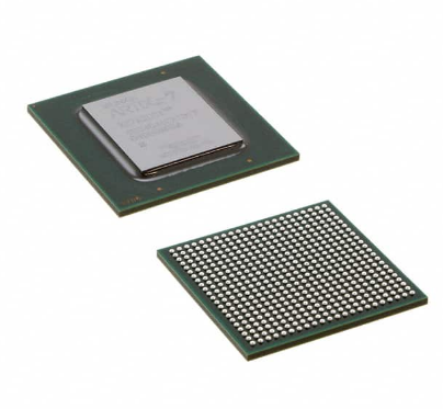
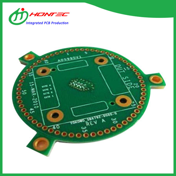
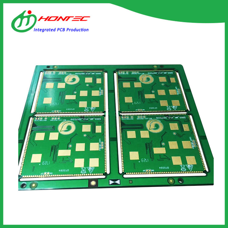
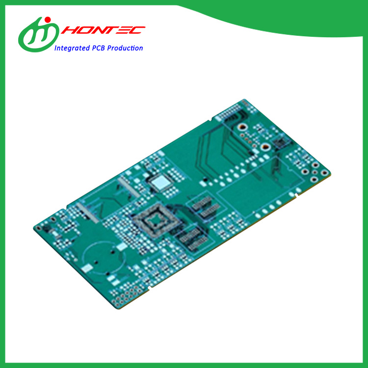
We always think and practice corresponding to the change of circumstance, and grow up. We goal at the achievement of a richer mind and body and also the living for Cross Blind Buried Hole PCB,Laser Blind Buried Hole PCB,4-layer via-in-PAD PCB,VIA-in-PAD PCB,VIA in PAD PCB, Make sure you sense absolutely absolutely free to speak to us for organization. nd we believe we are going to share the ideal trading practical experience with all our merchants.
Cross Blind Buried Hole PCB, Many kinds of different goods are available for you to choose, you can do one-stop shopping here. And customized orders are acceptable. Real business is to get win-win situation, if possible, we would like to provide more support for customers. Welcome all nice buyers communicate details of products with us!!

Hot Products

  • XCZU2CG-1SFVC784I

    XCZU2CG-1SFVC784I

    XCZU2CG-1SFVC784I is suitable for use in a variety of applications, including industrial control, telecommunications, and automotive systems. The device is known for its easy-to-use interface, high efficiency, and thermal performance, making it an ideal choice for a wide range of power management applications.
  • AD8041AN

    AD8041AN

    AD8041AN is suitable for use in a variety of applications, including industrial control, telecommunications, and automotive systems. The device is known for its easy-to-use interface, high efficiency, and thermal performance, making it an ideal choice for a wide range of power management applications.
  • XC7VX690T-3FFG1157E

    XC7VX690T-3FFG1157E

    XC7VX690T-3FFG1157E is suitable for use in a variety of applications, including industrial control, telecommunications, and automotive systems. The device is known for its easy-to-use interface, high efficiency, and thermal performance, making it an ideal choice for a wide range of power management applications.
  • XC3S400AN-4FGG400I

    XC3S400AN-4FGG400I

    XC3S400AN-4FGG400I is a low-cost field-programmable gate array (FPGA) developed by Intel Corporation, a leading semiconductor technology company. This device features 120,000 logic elements and 414 user input/output pins, making it suitable for a wide range of low-power and low-cost applications. It operates on a single power supply voltage ranging from 1.14V to 1.26V and supports various I/O standards such as LVCMOS, LVDS, and PCIe. The device has a maximum operating frequency of up to 415 MHz. The device comes in a small fine pitch ball grid array (FGBA) package with 484 pins, providing high pin-count connectivity for a variety of applications.
  • 10AX115R3F40E2SG

    10AX115R3F40E2SG

    10AX115R3F40E2SG is suitable for use in a variety of applications, including industrial control, telecommunications, and automotive systems. The device is known for its easy-to-use interface, high efficiency, and thermal performance, making it an ideal choice for a wide range of power management applications.
  • BCM82328FB1KFSBG

    BCM82328FB1KFSBG

    BCM82328FB1KFSBG is suitable for use in a variety of applications, including industrial control, telecommunications, and automotive systems. The device is known for its easy-to-use interface, high efficiency, and thermal performance, making it an ideal choice for a wide range of power management applications.

Send Inquiry