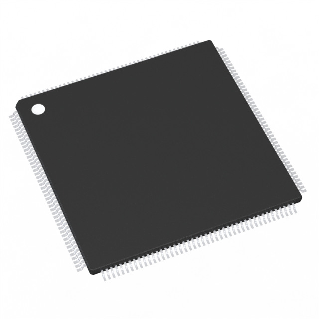
In the realm of miniaturized electronics where space is measured in microns and performance cannot be compromised, the substrate material and thickness become defining factors. The Ultra-thin BT PCB has emerged as the preferred platform for applications demanding exceptional dimensional stability, superior electrical properties, and minimal thickness. HONTEC has established itself as a trusted manufacturer of Ultra-thin BT PCB solutions, serving high-tech industries across 28 countries with specialized expertise in high-mix, low-volume, and quick-turn prototype production.
BT epoxy resin, or bismaleimide triazine, offers a unique combination of properties that make it ideal for thin-profile applications. With high glass transition temperature, low moisture absorption, and excellent dimensional stability, Ultra-thin BT PCB construction supports fine-pitch component assembly and maintains reliability under thermal cycling. Applications ranging from mobile devices and wearable electronics to semiconductor packaging and advanced sensor systems increasingly depend on Ultra-thin BT PCB technology to meet aggressive size and performance targets.
Located in Shenzhen, Guangdong, HONTEC combines advanced manufacturing capabilities with rigorous quality standards. Every Ultra-thin BT PCB produced carries the assurance of UL, SGS, and ISO9001 certifications, while the company actively implements ISO14001 and TS16949 standards. With logistics partnerships that include UPS, DHL, and world-class freight forwarders, HONTEC ensures efficient global delivery. Every inquiry receives a response within 24 hours, reflecting a commitment to responsiveness that global engineering teams value.
BT epoxy resin possesses a combination of material properties that make it exceptionally well-suited for Ultra-thin BT PCB fabrication. The high glass transition temperature of BT material, typically ranging from 180°C to 230°C, ensures that the substrate maintains mechanical integrity and dimensional stability even under elevated temperatures encountered during assembly and operation. This high Tg characteristic is particularly valuable for thin boards, as thinner substrates are inherently more susceptible to warpage and dimensional changes under thermal stress. The low moisture absorption of BT material, typically below 0.5%, prevents the dimensional instability and dielectric property shifts that can occur when hygroscopic materials absorb moisture. For Ultra-thin BT PCB designs, this stability translates to consistent impedance control and reliable fine-pitch component assembly. The coefficient of thermal expansion of BT closely matches that of silicon, reducing mechanical stress on solder joints when boards undergo thermal cycling—a critical consideration for thin boards that have less material to absorb thermal expansion forces. Additionally, BT material exhibits excellent dielectric properties with low dissipation factor, supporting high-frequency signal integrity even in thin constructions. HONTEC leverages these material advantages to deliver Ultra-thin BT PCB products that maintain reliability and electrical performance across demanding applications.
Fabricating Ultra-thin BT PCB products requires specialized processes that address the unique challenges of handling and processing thin, delicate substrates. HONTEC employs dedicated handling systems designed specifically for thin-board processing, including automated panel support systems that prevent flexing and stress during fabrication. The imaging process for thin BT substrates utilizes low-tension handling and precision alignment systems that maintain registration accuracy across the board surface without inducing distortion. Etching processes are optimized for the thin copper cladding typically used with BT materials, with controlled chemistry and conveyor speeds that achieve clean trace definition without over-etching. Lamination of Ultra-thin BT PCB constructions employs press cycles with carefully controlled pressure profiles that prevent resin flow irregularities while ensuring complete bonding between layers. Laser drilling, rather than mechanical drilling, is utilized for via formation in many thin BT applications, as laser processes provide the precision required for small via diameters without exerting mechanical stress that could damage thin materials. HONTEC implements additional quality checks specifically for thin boards, including warpage measurement, surface profile analysis, and enhanced optical inspection that detects defects that might be more critical in thin constructions. This specialized approach ensures that Ultra-thin BT PCB products meet the stringent quality requirements of compact electronic assemblies.
Ultra-thin BT PCB technology delivers maximum value in applications where space constraints, electrical performance, and reliability converge. Semiconductor packaging represents one of the largest application areas, with Ultra-thin BT PCB serving as substrate for chip-scale packages, system-in-package modules, and advanced memory devices. The thin profile and stable electrical properties of BT material support the fine lines and tight tolerances required for high-density interconnect in packaging applications. Mobile devices, including smartphones, tablets, and wearables, utilize Ultra-thin BT PCB construction for antenna modules, camera modules, and display interfaces where space is at a premium and signal integrity cannot be compromised. Medical devices, particularly implantable and wearable applications, benefit from the biocompatibility, thin profile, and reliability of BT substrates. HONTEC advises clients on design considerations specific to thin BT fabrication, including trace width and spacing requirements for different copper weights, via design rules for thin materials, and panelization strategies that optimize yield while maintaining board flatness. The engineering team also provides guidance on impedance control for thin constructions, where dielectric thickness variations have proportionally greater impact on characteristic impedance than in thicker boards. By addressing these considerations during design, clients achieve Ultra-thin BT PCB solutions that realize the full benefits of BT material while maintaining manufacturability and reliability.
HONTEC maintains manufacturing capabilities spanning the full range of Ultra-thin BT PCB requirements. Finished board thicknesses from 0.1mm to 0.8mm are supported, with layer counts appropriate to design complexity and thickness constraints. Copper weights from 0.25 oz to 1 oz accommodate fine-pitch routing and current-carrying requirements within thin profiles.
Surface finish selections for Ultra-thin BT PCB applications include ENIG for flat surfaces that support fine-pitch component assembly, immersion silver for solderability requirements, and ENEPIG for applications requiring wire bonding compatibility. HONTEC supports advanced via structures including microvias and filled vias that maintain surface flatness for component placement.
For engineering teams seeking a manufacturing partner capable of delivering reliable Ultra-thin BT PCB solutions from prototype through production, HONTEC offers technical expertise, responsive communication, and proven quality systems backed by international certifications.

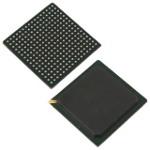
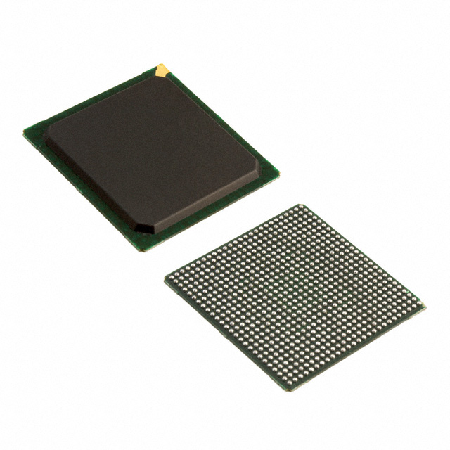
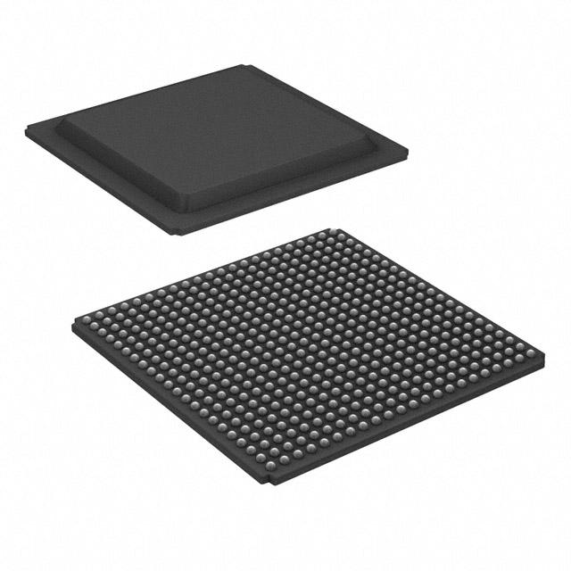
The IC carrier board is mainly used to carry the IC, and there are lines inside to conduct the signal between the chip and the circuit board. In addition to the function of the carrier, the IC carrier board also has a protection circuit, a dedicated line, a heat dissipation path, and a component module. Standardization and other additional functions.

ultra-thin BT PCB--Solid State Drive (Solid State Disk or Solid State Drive, referred to as SSD), commonly known as solid state drive, solid state drive is a hard disk made of solid state electronic storage chip array, because the solid state capacitor in Taiwan English is called Solid.The following is about Ultra Thin SSD Card PCB related, I hope to help you better understand Ultra Thin SSD Card PCB.