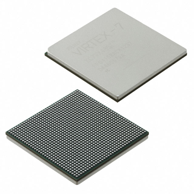
Wiring is the most important process in the entire PCB design. This will directly affect the performance of the PCB board. In the PCB design process, there are generally three such divisions of wiring: the first is routing, then the most basic requirements in PCB design. If none of the lines are routed and you can get flying lines everywhere, it will be an unqualified board. The second is the satisfaction of electrical performance. This is a measure of whether a printed circuit board is qualified. This is after wiring, carefully adjust the wiring so that it can achieve the best electrical performance. Then comes the beauty. If your wiring is laid, there is nothing to affect the performance of electrical appliances, but at first glance the messy past, plus the colorful, colorful, then how good your electrical performance, in the eyes of others is still a piece of garbage. This brings great inconvenience to testing and maintenance. The wiring should be neat and uniform, and can not be crisscrossed and unruly. These must be achieved under the condition of ensuring the performance of electrical appliances and meeting other individual requirements, otherwise it will be a waste of money. The wiring is mainly carried out according to the following principles:
①. Under normal circumstances, the power cord and ground wire should be wired first to ensure the electrical performance of the circuit board. To the extent possible, widen the width of the power and ground wires as much as possible. It is better that the ground wire is wider than the power wire. Their relationship is: ground wire> power wire> signal wire, usually the signal wire width is: 0.2 ~ 0.3mm , The thinnest width can reach 0.05~0.07mm, the power cord is generally 1.2~2.5mm. For the digital circuit PCB, a wide ground wire can be used to form a loop, that is, a ground network is used (the analog circuit ground cannot be used in this way)
②. Route the more stringent requirements (such as high-frequency lines) in advance, and the side lines of the input and output terminals should avoid adjacent parallel to avoid reflection interference. Ground wire isolation should be added when necessary, and the wiring of two adjacent layers should be perpendicular to each other, and parasitic coupling is likely to occur in parallel.
③. The oscillator case is grounded, the clock line should be as short as possible, and can not be led everywhere. The area of the special high-speed logic circuit under the clock oscillation circuit should increase the area of the ground, and should not take other signal lines to make the surrounding electric field approach zero;
④. As far as possible, use 45º polyline wiring. Do not use 90º polyline to reduce the radiation of high-frequency signals; (requires high lines to use double arcs)
⑤. Do not form a loop on any signal line. If it is inevitable, the loop should be as small as possible; the vias of the signal line should be as few as possible;
⑥. The key line should be as short and thick as possible, and add protective grounds on both sides.
⑦. When transmitting the sensitive signal and the noise field band signal through the flat cable, the "ground wire-signal-ground wire" method should be used.
⑧. Test points should be reserved for key signals to facilitate production and maintenance testing
⑨. After the schematic wiring is completed, the wiring should be optimized; at the same time, after the preliminary network check and DRC check are correct, fill the unrouted area with a ground wire, use a large area copper layer for the ground wire, and put it on the printed board. The places used are all connected to the ground as a ground wire. Or it can be made into a multi-layer board, and the power supply and ground wire each occupy one layer.