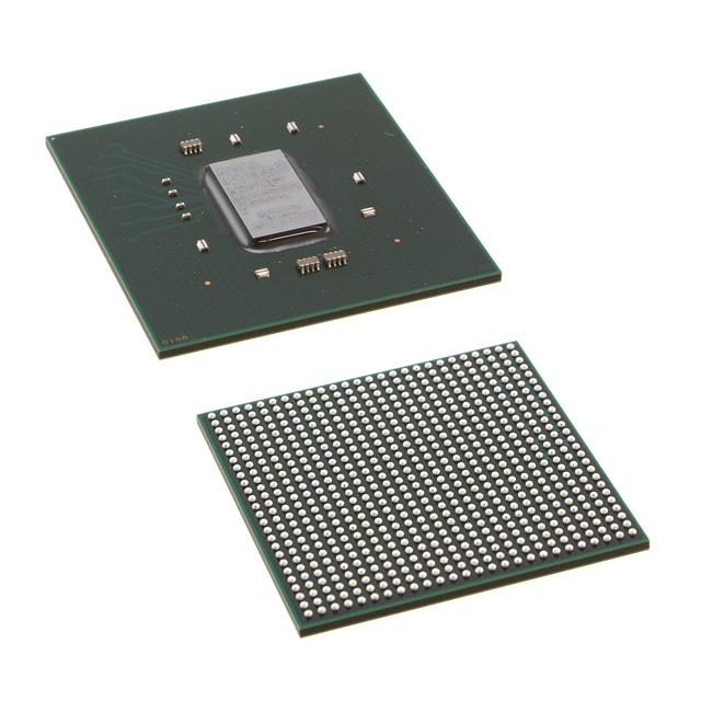
PCB Specification
A PCB may be a ticking bomb
When you order PCBs from the HONTEC, you are buying quality that pays for itself over time. This is guaranteed through a product specification and quality control that is far more stringent than other suppliers, and ensures that the product delivers what it promises.
Quality pays for itself in the long run even if not apparent at first sight
At first sight, PCBs differ little in appearance, irrespective of their inherent quality. It is under the surface that we focus on the differences so critical to the PCBs' durability and functionality. Customers cannot always see the difference, but they can rest assured that HONTEC puts a great deal of effort into ensuring that in turn, their customers are also supplied with PCBs that meet the most stringent quality standards.
It is vital that PCBs function reliably both during the manufacturing assembly process and, out in the field. Apart from the costs involved, faults during assembly can end up being built into the final product via the PCBs, with possible failure in the field resulting in compensation claims. Relative to that, in our opinion, the cost of a premium quality PCB is negligible.In all market sectors, particularly those producing products with critical applications, the consequences of such failures could be devastating.
Such aspects should be borne in mind when comparing PCB prices. Reliability and a guaranteed/long life cycle involve an initially higher outlay, but will pay for themselves in the long run.
HONTEC PCB SPECIFICATION, BEYOND IPC CLASS 2,12 of the 103 most important features of a durable PCB
1) 25 micron nominal hole plating as per IPC class 3
BENEFITS:Increased reliability including improved z-axis expansion resistance.
RISK OF NOT HAVING:Blow holes or outgassing, electrical continuity problems (inner layer separation, barrel cracking) during assembly or risk of field failures under load conditions. IPC Class 2 (standard for most factories) provides 20% less copper.
• No track welding or open circuit repair
BENEFITS:Reliability through perfect circuitry and security as no repair = no risk.
RISK OF NOT HAVING:Poor repair can actually lead to open circuits being supplied. Even a ‘good' repair has a risk of failure under load conditions (vibration etc.) leading to potential field failures.
2) Cleanliness requirements beyond those of IPC
BENEFITS:Improved cleanliess of the PCB influences increased reliability.
RISK OF NOT HAVING:Residues on the boards, solder pick up, risk of conformal coating problems, ionic residues leading to risk of corrosion and contamination of the surfaces which are used for soldering – both potentially leading to reliability issues (poor solder joint / electrical failures) and ultimately increased potential for field failures.
3) Tight control on age of specific finishes
BENEFITS:Solderability, reliability and less risk of moisture ingression.
RISK OF NOT HAVING:Solderability problems can occur as a result of metallurgical changes within the finish of old boards, whilst moisture ingression can lead to delamination, inner layer separation (open circuits) during assembly and/or when in the field.
• Internationally known base materials used – no ‘local' or unknown brands allowed
BENEFITS:Increased reliability and known performance.
RISK OF NOT HAVING:Poor mechanical properties mean the board doesn't behave as expected during assembly conditions – for example: higher expansion properties leading to delamination / open circuits and also warpage problems. Reduced electrical characteristics can lead to poor impedance performance.
• Tolerance for copper clad laminate is IPC4101 class B/L
BENEFITS:Tighter control of dielectric spacing provides less deviation in electrical performance expectations.
RISK OF NOT HAVING:Electrical characteristics may not be exactly as planned and units within the same batch can demonstrate greater variation in output / performance.
• Defined soldermasks and ensuring accordance to IPC-SM-840 class T
BENEFITS:HONTEC approves ‘good' materials to provide security in the ink and in knowing the soldermasks are covered within UL approvals.
RISK OF NOT HAVING:Poor inks can lead to problems with adhesion, resistance to solvents and hardness – all of which can see soldermask coming away from the board ultimately leading to corrosion of the copper circuitry. Poor insulation characteristics can lead to short circuits through unwanted electrical continuity / arcing.
• Defined tolerances for profile, holes and other mechanical features
BENEFITS:Tighter tolerances means improved dimensional quality of the product – better fit, form and function.
RISK OF NOT HAVING:Problems during assembly such as alignment / fit (press fit pin problems that are only found when the unit is fully assembled). Also problems with assembly into any housing due to increased deviation in dimensions.
• HONTEC specifies soldermask thickness – IPC does not
BENEFITS:Better electrical insulation, less risk of flaking or loss adhesion and greater resilient to mechanical impact – wherever that may happen!
RISK OF NOT HAVING:Thin deposits of soldermask can lead to problems with adhesion, resistance to solvents and hardness – all of which can see soldermask coming away from the board ultimately leading to corrosion of copper circuitry. Poor insulation characteristics due to the thin deposit can lead to short circuits through unwanted electrical continuity / arcing.
• HONTEC defines cosmetic and repair requirements – IPC does not
BENEFITS:Security as a result of love and care during the manufacturing process.
RISK OF NOT HAVING:Multiple scratches, minor damage, touch ups and repairs – a functional but perhaps unsightly board. If concerned over what can be seen, then what risks are involved with what cannot be seen, and the potential impact on assembly or risk when in the field??
• Specific requirements of depth of via fill
BENEFITS:A good quality filled via hole will provide less risk of rejection during the assembly process.
RISK OF NOT HAVING:Half filled via holes may trap chemical residues from the ENIG process which can cause problems such as solderability. Such via holes can also trap solderballs within the hole which can escape and cause short circuits either during assembly or in the field.
• Peters SD2955 peelable as standard
BENEFITS:The benchmark for peelable mask – no ‘local' or cheap brands.
RISK OF NOT HAVING:Poor or cheap peelable can blister, melt, tear or simply set like concrete during assembly so that the peelable does not peel / does not work.
Surface Finishes
A surface finish can be either organic or metallic in nature. Comparing both types and all available options can quickly demonstrate the relative benefits or drawbacks. Typically, the decisive factors when it comes to selecting the most suitable finish is the end application, the assembly process and the design of the PCB itself. Below you can find a brief summary of the most common finishes, however for further or more detailed information, please contact HONTEC and we will be more than happy to answer any of your questions.
|
HASL – Tin/Lead hot air solder level |
|
|
|
• Excellent solderability • Inexpensive / Low cost • Allows large processing window • Long industry experience / well known finish • Multiple thermal excursions |
|
|
• Difference in thickness / topography between large and small pads • Not suited for < 20mil pitch SMD & BGA • Bridging on fine pitch • Not ideal for HDI products |
|
|
|
|
LF HASL – Lead Free hot air solder level |
|
|
|
• Excellent solderability • Relatively inexpensive • Allows large processing window • Multiple thermal excursions |
|
|
• Difference in thickness / topography between large and small pads – but to a lesser degree than SnPb • High processing temperature – 260-270 degrees C • Not suited for < 20mil pitch SMD & BGA • Bridging on fine pitch • Not ideal for HDI products |
|
|
|
|
ENIG – Immersion gold / Electroless Nickel Immersion Gold |
|
|
|
• Immersion finish = excellent flatness • Good for fine pitch / BGA / smaller components • Tried and tested process • Wire bondable |
|
|
• Expensive finish • Black pad concerns on BGA • Can be aggressive to soldermask – larger soldermask dam preferred • Avoid soldermask defined BGA's • Should not plug holes on one side only |
|
|
|
|
Immersion Sn – Immersion Tin |
|
|
|
• Immersion finish = excellent flatness • Good for fine pitch / BGA / smaller components • Mid range cost for lead free finish • Press fit suitable finish • Good solderability after multiple thermal excursions |
|
|
• Very sensitive to handling – gloves must be used • Tin whisker concerns • Aggressive to soldermask – soldermask dam shall be ≥ 5 mil • Baking prior to use can have a negative effect • Not recommended to use peelable masks • Should not plug holes on one side only |
|
|
|
|
Immersion Ag – Immersion Silver |
|
|
|
• Immersion finish = excellent flatness • Good for fine pitch / BGA / smaller components • Mid range cost for lead free finish • Can be reworked |
|
|
• Very sensitive to handling / tarnishing / cosmetic concerns – gloves must be used • Special packaging required – if packaged opened and not all boards used, it must be resealed quickly. • Short operating window between assembly stages • Not recommended to use peelable masks • Should not plug holes from one side only • Reduced supply chain options to support this finish |
|
|
|
|
OSP (Organic Solderability Preservative) |
|
|
|
• Excellent flatness • Good for fine pitch / BGA / smaller components • Inexpensive / Low cost • Can be reworked • Clean, environmentally friendly process |
|
|
• Very sensitive to handling – gloves must be used and scratches avoided • Short operating window between assembly stages • Limited thermal cycles so not preferred for multiple soldering processes (>2/3) • Limited shelf life – not ideal for specific freight modes and long stock holding • Very difficult to inspect • Cleaning misprinted solderpaste can have a negative effect on the OSP coating • Baking prior to use can have a negative effect |