In the convergence of optical and electronic technologies, the interface between light-based components and traditional circuitry demands specialized design considerations. The Optoelectronic PCB provides the essential platform for integrating lasers, photodetectors, optical transceivers, and display elements with supporting electronic circuits. HONTEC has established itself as a trusted manufacturer of Optoelectronic PCB solutions, serving high-tech industries across 28 countries with specialized expertise in high-mix, low-volume, and quick-turn prototype production.
The Optoelectronic PCB differs significantly from conventional circuit boards in its material selection, surface finish requirements, and fabrication precision. Applications ranging from fiber optic communication systems and LiDAR sensors to medical imaging equipment and high-brightness LED arrays demand the unique capabilities that Optoelectronic PCB technology provides. These boards must accommodate both high-speed electronic signals and precise optical alignment, often within the same compact assembly.
Located in Shenzhen, Guangdong, HONTEC combines advanced manufacturing capabilities with rigorous quality standards. Every Optoelectronic PCB produced carries the assurance of UL, SGS, and ISO9001 certifications, while the company actively implements ISO14001 and TS16949 standards. With logistics partnerships that include UPS, DHL, and world-class freight forwarders, HONTEC ensures efficient global delivery. Every inquiry receives a response within 24 hours, reflecting a commitment to responsiveness that global engineering teams value.
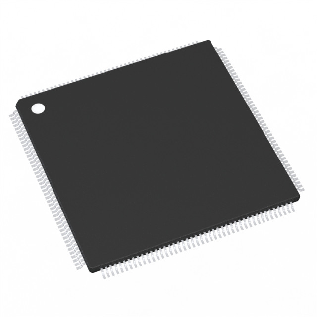
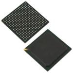
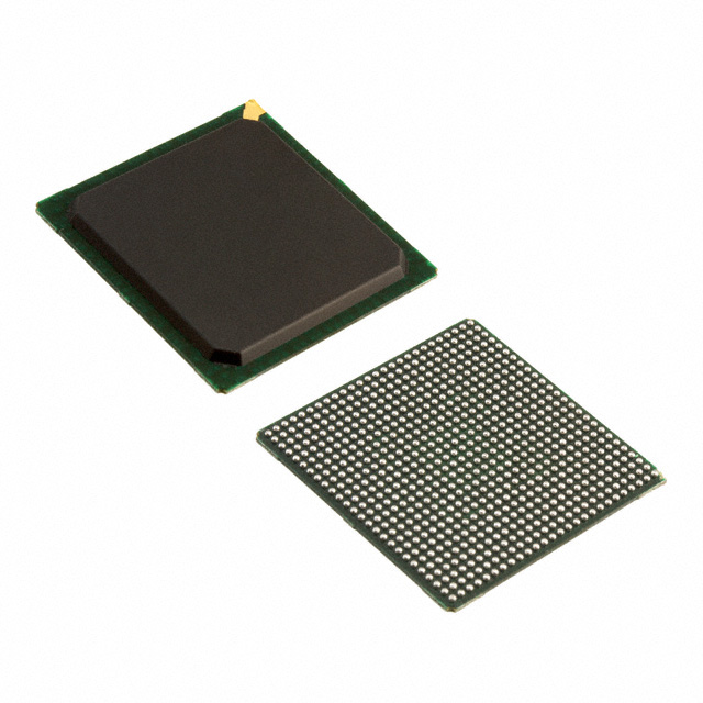
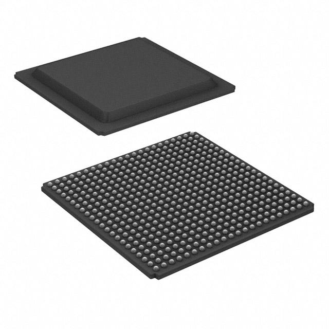
The Optoelectronic PCB differs from standard PCB constructions in several critical aspects that reflect the unique requirements of optical component integration. Material selection represents the most fundamental difference. While standard PCBs typically utilize FR-4 laminates, Optoelectronic PCB designs often require materials with specific optical properties, such as high reflectivity for LED applications or low optical absorption for transparent waveguides. Surface finish requirements also diverge significantly. Standard PCB surface finishes prioritize solderability and wire bond compatibility, but Optoelectronic PCB finishes must additionally provide high reflectivity for light extraction from LEDs or precise gold surfaces for flip-chip attachment of vertical-cavity surface-emitting lasers. Dimensional stability requirements are substantially tighter for Optoelectronic PCB applications, as optical alignment tolerances typically measure in microns rather than the hundredths of millimeters acceptable for standard electronic assemblies. The board must maintain flatness and positional accuracy through thermal cycling to preserve optical coupling efficiency. Thermal management considerations are amplified in Optoelectronic PCB designs, as optoelectronic components often generate concentrated heat that must be efficiently extracted to maintain wavelength stability and device longevity. HONTEC works with clients to select materials, finishes, and fabrication processes that align with the specific optical and electronic requirements of each application.
Maintaining the tight tolerances required for optical alignment in Optoelectronic PCB fabrication demands precision manufacturing capabilities that exceed standard PCB requirements. HONTEC employs laser direct imaging systems that achieve registration accuracy within 0.015mm across the entire board surface, ensuring that fiducial marks, bond pads, and alignment features maintain their designed relative positions. For Optoelectronic PCB designs incorporating cavities or recessed features for optical component placement, HONTEC utilizes precision routing and controlled-depth machining that achieves depth tolerances within ±0.05mm. The lamination process for multilayer Optoelectronic PCB constructions employs specialized press cycles that maintain board flatness critical for optical alignment, with post-lamination leveling processes applied where required. Plating thickness uniformity receives particular attention, as variations in gold or copper thickness on optical interface surfaces can affect light coupling efficiency and component attachment. HONTEC performs comprehensive dimensional verification using coordinate measurement systems that validate critical feature positions relative to established datums. Thermal cycling testing confirms that the Optoelectronic PCB maintains dimensional stability across operating temperature ranges, ensuring that alignment established at assembly remains intact during field operation. This systematic approach to precision manufacturing enables Optoelectronic PCB products that meet the exacting requirements of optical-electronic integration.
Optoelectronic PCB technology delivers maximum value in applications requiring seamless integration of optical and electronic functions. Fiber optic communication systems represent a primary application area, where Optoelectronic PCB construction supports optical transceivers, modulators, and receiver assemblies within compact form factors. The boards must provide precise alignment for fiber attachment while maintaining high-speed signal integrity for the electronic interface. LiDAR sensors for automotive and industrial applications utilize Optoelectronic PCB technology to integrate laser emitters, photodetectors, and processing electronics within unified assemblies that must maintain optical alignment under vibration and temperature extremes. Medical imaging and diagnostic equipment, including endoscopes and optical coherence tomography systems, depend on Optoelectronic PCB designs that combine miniature optical components with sensitive electronic circuitry within space-constrained housings. HONTEC advises clients on design considerations specific to optoelectronic integration, including thermal management strategies that maintain optical component wavelength stability, electrical isolation between sensitive optical receivers and noisy power circuits, and mechanical design that protects optical interfaces during assembly and field service. The engineering team also provides guidance on material selection for different optical wavelengths, as materials that are transparent or reflective at one wavelength may behave differently at another. By addressing these considerations during design, clients achieve Optoelectronic PCB solutions that optimize optical performance, electrical functionality, and long-term reliability.
HONTEC maintains manufacturing capabilities spanning the full range of Optoelectronic PCB requirements. Surface finish options include ENIG for consistent solderability, ENEPIG for wire bonding compatibility, and selective hard gold for contact interfaces. Cavity creation capabilities support recessed component placement for optical alignment.
Board constructions incorporate materials selected for optical performance, including white solder masks for LED reflectivity, black solder masks for contrast in display applications, and specialty laminates with controlled optical properties. HONTEC supports high-frequency materials for optoelectronic applications requiring high-speed signal integrity alongside optical functionality.
For engineering teams seeking a manufacturing partner capable of delivering reliable Optoelectronic PCB solutions from prototype through production, HONTEC offers technical expertise, responsive communication, and proven quality systems backed by international certifications.

800G optical module PCB - at present, the transmission rate of global optical network is rapidly moving from 100g to 200g / 400g. In 2019, ZTE, China Mobile and Huawei respectively verified in Guangdong Unicom that single carrier 600g can achieve 48tbit / s transmission capacity of single fiber.

The 200G optical module PCB is composed of shell, PCBA (PCB blank board + driver chip) and optical devices (dual fiber: Tosa, Rosa; single fiber: Bosa). In short, the function of the optical module is photoelectric conversion. The transmitter converts the electrical signal into the optical signal, and then the receiver converts the optical signal into the electrical signal after transmission through the optical fiber.

100G optoelectronic PCB is a packaging substrate for a new generation of high computing, which integrates light with electricity, transmits signals with light and operates with electricity. It adds a layer of light guide to the traditional printed circuit board, which is very mature at present.

The pace of the 400g network is getting closer and closer. The domestic Internet giants Alibaba and Tencent plan to start upgrading the 400g network in 2019. The 400G optical module PCB, as the hardware of the 400G network upgrade, has attracted the attention of all parties.

The main function of 40G optical module PCB is to realize photoelectric and electro-optic transformation, including optical power control, modulation and transmission, signal detection, IV conversion and limiting amplification judgment regeneration. In addition, there are anti-counterfeiting information query, TX disable and other functions. The common functions are: SFF, SFF, GBP +, GBIC, XFP, 1x9, etc.

The function of the Optical module PCB is to convert the electrical signal into optical signal at the sending end, and then convert the optical signal into the electrical signal at the receiving end after transmitting through the optical fiber.