In high-power electronic systems where heat dissipation determines reliability and performance, conventional thermal management approaches often fall short. The Inlaid Copper Coin PCB represents a specialized solution designed to extract heat directly from power-dense components, providing a direct thermal pathway that dramatically reduces operating temperatures. HONTEC has established itself as a trusted manufacturer of Inlaid Copper Coin PCB solutions, serving high-tech industries across 28 countries with specialized expertise in high-mix, low-volume, and quick-turn prototype production.
The Inlaid Copper Coin PCB technology addresses one of the most persistent challenges in power electronics: efficiently removing heat from components that generate significant thermal energy. By embedding solid copper coins directly into the PCB structure beneath critical components, this construction creates a low-thermal-resistance path that conducts heat away from the component junction and into the board’s thermal management system. Applications ranging from high-power LED arrays and automotive power modules to RF power amplifiers and industrial motor drives increasingly depend on Inlaid Copper Coin PCB technology to achieve reliable operation under demanding thermal conditions.
Located in Shenzhen, Guangdong, HONTEC combines advanced manufacturing capabilities with rigorous quality standards. Every Inlaid Copper Coin PCB produced carries the assurance of UL, SGS, and ISO9001 certifications, while the company actively implements ISO14001 and TS16949 standards. With logistics partnerships that include UPS, DHL, and world-class freight forwarders, HONTEC ensures efficient global delivery. Every inquiry receives a response within 24 hours, reflecting a commitment to responsiveness that global engineering teams value.
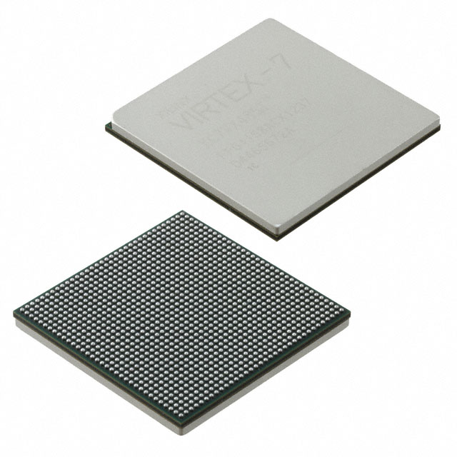
An Inlaid Copper Coin PCB is a specialized circuit board construction where solid copper coin elements are embedded into the board structure, positioned directly beneath heat-generating components. This differs fundamentally from standard thermal management approaches such as thermal vias or copper pours. Traditional thermal vias rely on arrays of plated holes to conduct heat through the board, but the thermal conductivity of plated copper within vias is limited by the thin copper layer on via walls, and air gaps within vias create additional thermal resistance. Copper pours on inner layers provide some heat spreading but still rely on the relatively low thermal conductivity of dielectric materials between the component and the copper. An Inlaid Copper Coin PCB places a solid copper mass directly under the component, creating a continuous metal path with minimal thermal resistance. The copper coin, typically ranging from 0.5mm to 2.0mm in thickness, provides a direct thermal conduit that efficiently transfers heat from the component mounting pad through the board to the opposite side, where it can be dissipated by a heatsink or other cooling solution. HONTEC works with clients to determine optimal coin dimensions, placement, and integration methods based on component power dissipation, available board space, and overall thermal management requirements.
The integration of copper coins into a Inlaid Copper Coin PCB requires specialized fabrication processes that ensure mechanical stability, electrical isolation where required, and long-term reliability. HONTEC employs precision machining to create cavities within the PCB laminate that accommodate the copper coin with controlled clearances. The copper coin itself is fabricated from high-purity copper selected for its thermal conductivity, with surface finishes applied to promote adhesion and solderability. During lamination, specialized press cycles and materials are used to bond the coin securely within the cavity while maintaining the integrity of surrounding circuit features. For designs requiring electrical isolation between the coin and surrounding circuits, HONTEC utilizes dielectric materials that separate the coin from conductive layers while maintaining thermal transfer. Plating processes ensure that the coin surface remains coplanar with the board surface, providing a flat mounting surface for component attachment. HONTEC performs cross-section analysis on Inlaid Copper Coin PCB products to verify coin alignment, cavity fill, and interface integrity. Thermal cycling testing validates that the interface between the coin and surrounding materials maintains structural integrity across operating temperature ranges. This comprehensive approach ensures that the Inlaid Copper Coin PCB delivers the expected thermal performance without compromising board reliability.
Implementing Inlaid Copper Coin PCB technology successfully requires design considerations that address both thermal performance and manufacturability. HONTEC engineering team emphasizes that coin placement is the most critical factor. The coin should be positioned directly beneath the component’s thermal pad, with dimensions that match or slightly exceed the component’s heat-generating area. For components with multiple thermal pads, individual coins or a single larger coin may be appropriate depending on layout constraints. Thermal interface between the component and the copper coin requires careful attention. HONTEC recommends solder attachment of components to the coin surface where possible, as solder provides excellent thermal conductivity. For applications requiring electrical isolation, thermal interface materials can be specified that provide electrical insulation while maintaining thermal transfer. The surrounding board design must accommodate the presence of the copper coin, with routing and component placement adjusted to maintain required clearances. HONTEC advises clients to consider the impact of the coin on overall board flatness, as differential thermal expansion between the coin and surrounding materials can induce stress during thermal cycling. The engineering team provides guidance on coin thickness selection, with thicker coins providing greater heat capacity and lower thermal resistance but also increasing overall board thickness and weight. By addressing these considerations during design, clients achieve Inlaid Copper Coin PCB solutions that optimize thermal performance while maintaining manufacturing viability.
HONTEC maintains manufacturing capabilities spanning the full range of Inlaid Copper Coin PCB requirements. Copper coin diameters from 3mm to 30mm are supported, with thicknesses ranging from 0.5mm to 2.5mm depending on application requirements. Single coin configurations serve localized hot spots, while multiple coin arrangements address designs with multiple power-dense components.
Board constructions incorporating Inlaid Copper Coin PCB technology range from simple 2-layer designs to complex multilayer boards with high-density routing. Material selections include standard FR-4 for general applications, high-Tg materials for enhanced thermal stability, and aluminum-backed substrates for applications requiring additional heat spreading.
For engineering teams seeking a manufacturing partner capable of delivering reliable Inlaid Copper Coin PCB solutions from prototype through production, HONTEC offers technical expertise, responsive communication, and proven quality systems backed by international certifications.

built-in Copper Coin PCB-- HONTEC uses prefabricated copper blocks to splice with FR4, then uses resin to fill and fix them, and then combines them perfectly by copper plating to connect them with the circuit copper

The Inlaid Copper Coin PCB is inlaid in the FR4, so as to achieve the function of heat dissipation of a certain chip. Compared with ordinary epoxy resin, the effect is remarkable.

The so-called Buried Copper Coin PCB is a PCB board in which a copper Coin is partially embedded on the PCB. The heating elements are directly attached to the surface of the copper Coin board, and the heat is transferred out through the copper Coin.