Laser Blind Buried Hole PCB Manufacturers

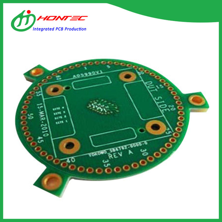
We believe that prolonged time period partnership is really a result of top of the range, benefit added provider, prosperous knowledge and personal contact for Laser Blind Buried Hole PCB,Cross Blind Buried Hole PCB,4-layer via-in-PAD PCB,VIA-in-PAD PCB,VIA in PAD PCB, we could solve our customer problems asap and do the profit for our customer. For those who need superior provider and excellent , pls choose us , thanks !
Laser Blind Buried Hole PCB, Our company now has many department, and there have more than 20 employees in our company. We set up sales shop, show room, and product warehouse. In the meantime, we registered our own brand. We have tightened inspection for quality of product.

Hot Products

  • XC6SLX45-2CSG484C

    XC6SLX45-2CSG484C

    XC6SLX45-2CSG484C is suitable for use in a variety of applications, including industrial control, telecommunications, and automotive systems. The device is known for its easy-to-use interface, high efficiency, and thermal performance, making it an ideal choice for a wide range of power management applications.
  • XCKU5P-L2FFVB676E

    XCKU5P-L2FFVB676E

    XCKU5P-L2FFVB676E is a high-performance FPGA (Field Programmable Gate Array) product launched by Xilinx. This FPGA belongs to the Kintex UltraScale+series and has the following features and specifications
  • EM-528K High-speed PCB

    EM-528K High-speed PCB

    EM-528K High-speed PCB is almost everywhere in our industry. And, as quoted, we always say that, regardless of the final product or implementation, each PCB is high-speed with its IC technology.
  • MCP4725A0T-E/CH

    MCP4725A0T-E/CH

    MCP4725A0T-E/CH is suitable for use in a variety of applications, including industrial control, telecommunications, and automotive systems. The device is known for its easy-to-use interface, high efficiency, and thermal performance, making it an ideal choice for a wide range of power management applications.
  • XC3S1500-4FGG676I

    XC3S1500-4FGG676I

    XC3S1500-4FGG676I is a low-cost field-programmable gate array (FPGA) developed by Intel Corporation, a leading semiconductor technology company. This device features 120,000 logic elements and 414 user input/output pins, making it suitable for a wide range of low-power and low-cost applications. It operates on a single power supply voltage ranging from 1.14V to 1.26V and supports various I/O standards such as LVCMOS, LVDS, and PCIe. The device has a maximum operating frequency of up to 415 MHz. The device comes in a small fine pitch ball grid array (FGBA) package with 484 pins, providing high pin-count connectivity for a variety of applications.
  • MTA18ASF4G72HZ-3G2F1

    MTA18ASF4G72HZ-3G2F1

    MTA18ASF4G72HZ-3G2F1 is suitable for use in a variety of applications, including industrial control, telecommunications, and automotive systems. The device is known for its easy-to-use interface, high efficiency, and thermal performance, making it an ideal choice for a wide range of power management applications.

Send Inquiry