The relentless push toward smaller, lighter, and more powerful electronic devices has redefined what engineers expect from printed circuit board technology. As consumer electronics, medical implants, automotive systems, and aerospace applications demand ever-higher component density within shrinking footprints, the HDI Board has become the standard for modern electronic design. HONTEC has established itself as a trusted manufacturer of HDI Board solutions, serving high-tech industries across 28 countries with specialized expertise in high-mix, low-volume, and quick-turn prototype production.
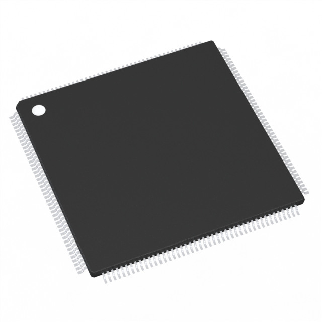
High Density Interconnect technology represents a fundamental shift in how circuits are constructed. Unlike traditional PCBs that rely on through-hole vias and standard trace widths, HDI Board construction utilizes microvias, fine lines, and advanced sequential lamination techniques to pack more functionality into less space. The result is a board that not only supports the latest high-pin-count components but also delivers improved signal integrity, reduced power consumption, and enhanced thermal performance.
Located in Shenzhen, Guangdong, HONTEC combines advanced manufacturing capabilities with rigorous quality standards. Every HDI Board produced carries the assurance of UL, SGS, and ISO9001 certifications, while the company actively implements ISO14001 and TS16949 standards to meet the demanding requirements of automotive and industrial applications. With logistics partnerships that include UPS, DHL, and world-class freight forwarders, HONTEC ensures that prototype and production orders reach destinations worldwide efficiently. Every inquiry receives a response within 24 hours, reflecting a commitment to responsiveness that global engineering teams have come to trust.
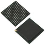
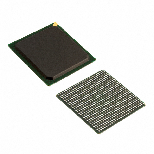
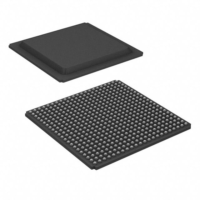
The distinction between HDI Board technology and conventional multilayer PCB construction lies primarily in the methods used to create interconnections between layers. Traditional multilayer boards rely on through-hole vias that drill completely through the entire stack, consuming valuable real estate and limiting routing density on inner layers. HDI Board construction utilizes microvias—laser-drilled holes typically ranging from 0.075mm to 0.15mm in diameter—that connect only specific layers rather than the entire board. These microvias can be stacked or staggered to create complex interconnection patterns that bypass the routing constraints of traditional designs. Additionally, HDI Board technology employs sequential lamination, where the board is built up in stages rather than laminated all at once. This allows for buried vias within inner layers and enables finer trace widths and spacing, typically down to 0.075mm or smaller. The combination of microvias, fine-line capabilities, and sequential lamination results in a HDI Board that can accommodate components with 0.4mm pitch or smaller while maintaining signal integrity and thermal performance. HONTEC works with clients to determine the appropriate HDI structure—whether Type I, II, or III—based on component requirements, layer count, and production volume considerations.
Reliability in HDI Board manufacturing demands exceptional process control, as the tight geometries and microvia structures leave little margin for error. HONTEC implements a comprehensive quality management system specifically designed for HDI fabrication. The process begins with laser drilling, where precision calibration ensures consistent microvia formation without damaging underlying pads. Copper filling of microvias utilizes specialized plating chemistries and current profiles that achieve complete fill without voids—a critical factor for long-term reliability under thermal cycling. Laser direct imaging replaces traditional photo tools for fine-line patterning, achieving registration accuracy within 0.025mm across the entire panel. HONTEC performs automated optical inspection at multiple stages, with particular focus on microvia alignment and fine-line integrity. Thermal stress testing, including multiple cycles of reflow simulation, validates that microvias maintain electrical continuity without separation. Cross-sectioning is performed on every production batch to verify microvia fill quality, copper thickness distribution, and layer registration. Statistical process control tracks key parameters including microvia aspect ratio, copper plating uniformity, and impedance variation, allowing early detection of process drift. This rigorous approach enables HONTEC to deliver HDI Board products that meet the reliability expectations of demanding applications including automotive electronics, medical devices, and portable consumer products.
Transitioning from traditional PCB architecture to HDI Board design requires a shift in design methodology that addresses several critical factors. HONTEC engineering team emphasizes that component placement strategy becomes more influential in HDI design, as microvia structures can be placed directly under components—a technique known as via-in-pad—which significantly reduces inductance and improves thermal dissipation. This capability allows designers to position decoupling capacitors closer to power pins and achieve cleaner power distribution. Stack-up planning requires careful consideration of the sequential lamination stages, as each lamination cycle adds time and cost. HONTEC advises clients to optimize layer count by utilizing microvias to reduce the number of layers required, often achieving the same routing density with fewer layers than conventional designs. Impedance control demands attention to the varying dielectric thicknesses that can occur between sequential lamination stages. Designers must also consider the aspect ratio limitations for microvias, typically maintaining a 1:1 depth-to-diameter ratio for reliable copper fill. Panel utilization influences cost, and HONTEC provides guidance on design panelization that maximizes efficiency while maintaining manufacturability. By addressing these considerations during the design phase, clients achieve HDI Board solutions that realize the full benefits of HDI technology—reduced size, enhanced electrical performance, and optimized manufacturing cost.
HONTEC maintains manufacturing capabilities that span the full spectrum of HDI Board complexity. Type I HDI boards utilize microvias on outer layers only, providing a cost-effective entry point for designs requiring moderate density improvement. Type II and Type III HDI configurations incorporate buried vias and multiple layers of sequential lamination, supporting the most demanding applications with component pitches below 0.4mm and routing densities that approach the physical limits of current technology.
Material selection for HDI Board fabrication includes standard FR-4 for cost-sensitive applications, as well as low-loss materials for designs requiring enhanced signal integrity at high frequencies. HONTEC supports advanced surface finishes including ENIG, ENEPIG, and immersion tin, with selections based on component requirements and assembly processes.
For engineering teams seeking a manufacturing partner capable of delivering reliable HDI Board solutions from prototype through production, HONTEC offers technical expertise, responsive communication, and proven quality systems. The combination of international certifications, advanced manufacturing capabilities, and a customer-focused approach ensures that every project receives the attention necessary for successful product development in an increasingly competitive landscape.

P0.75 LED PCB-Small spacing LED display refers to indoor LED display with LED dot spacing of P2 and below, mainly including P2, p1.875, p1.667, p1.47, p1.25, P1.0, p0.9, p0.75 and other LED display products. With the improvement of LED display manufacturing technology, the resolution of traditional LED display has been greatly improved.

EM-891K PCB is made of EM-891k material with the lowest loss of EMC brand by HONTEC. This material has the advantages of high speed, low loss and better performance.

The buried hole is not necessarily HDI. Large size HDI PCB first-order and second-order and third-order how to distinguish the first-order is relatively simple, the process and process are easy to control. Second order began to trouble, one is the problem of alignment, a hole and copper plating problem.

TU-943N PCB is the abbreviation of high density interconnection. It is a kind of printed circuit board (PCB) production. It is a circuit board with high line distribution density using micro blind buried hole technology. EM-888 HDI PCB is a compact product designed for small capacity users.

ELIC HDI PCB printed circuit board is the use of the latest technology to increase the use of printed circuit boards in the same or smaller area. This has driven major advances in mobile phone and computer products, producing revolutionary new products. This includes touch-screen computers and 4G communications and military applications, such as avionics and intelligent military equipment.

Half-hole PCB is a compact product designed for small capacity users. It adopts modular parallel design, with a module capacity of 1000VA (height of 1U), natural cooling, and can be directly put into a 19 "rack, with a maximum of 6 modules in parallel. The product adopts full digital signal processing (DSP) technology and a number of patent technologies. It has a full range of load adaptability and strong short-term overload capacity, and can not consider the load power factor and peak factor.