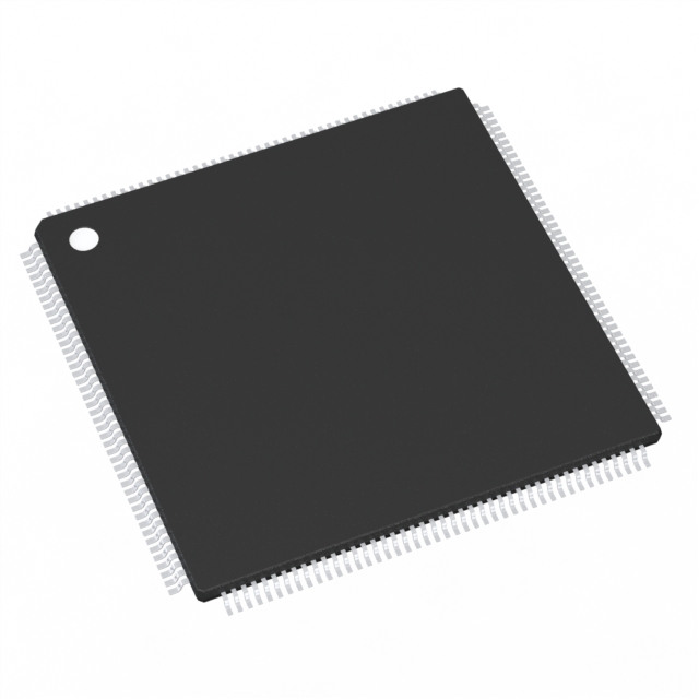
In industries where size matters as much as performance, the ability to produce reliable circuit boards in expansive dimensions is essential. From LED lighting panels and industrial control systems to medical imaging equipment and aerospace instrumentation, Large Size PCB technology enables applications that simply cannot fit within standard board dimensions. HONTEC has established itself as a trusted manufacturer of Large Size PCB solutions, serving high-tech industries across 28 countries with specialized expertise in high-mix, low-volume, and quick-turn prototype production.
The demand for Large Size PCB continues to grow as systems become more integrated and form factors expand. These boards, often exceeding 600mm in length or width, require specialized handling, precise process controls, and manufacturing equipment capable of maintaining quality across extended dimensions. HONTEC combines advanced fabrication capabilities with rigorous quality standards to deliver Large Size PCB products that meet the most demanding specifications while maintaining the reliability expected from smaller format boards.
Located in Shenzhen, Guangdong, HONTEC operates with certifications including UL, SGS, and ISO9001, while actively implementing ISO14001 and TS16949 standards. The company partners with UPS, DHL, and world-class freight forwarders to ensure efficient global delivery. Every inquiry receives a response within 24 hours, reflecting a commitment to responsiveness that global engineering teams value.
A Large Size PCB is generally defined as any circuit board exceeding 600 millimeters on at least one dimension, though specific thresholds vary by manufacturer capability. HONTEC supports Large Size PCB configurations up to 1200mm in length, with panel sizes optimized for specific application requirements. Applications requiring Large Size PCB construction include LED lighting panels used in commercial and industrial installations, where seamless arrays demand extended board dimensions to minimize interconnection points and simplify installation. Industrial control systems for manufacturing equipment often utilize large format boards to accommodate numerous I/O interfaces, power distribution networks, and control circuitry within a unified platform. Medical imaging equipment, including diagnostic displays and scanning systems, requires Large Size PCB designs that support high-resolution imaging across expansive surfaces. Backplanes for telecommunications equipment and server infrastructure utilize large format construction to interconnect multiple daughter cards within rack-mounted systems. Aerospace and defense applications, including radar systems and avionics displays, demand Large Size PCB solutions that maintain reliability under stringent environmental conditions. HONTEC works with clients to evaluate dimensional requirements against panel utilization, handling considerations, and assembly constraints to optimize board sizing for each application.
Maintaining precision across Large Size PCB fabrication requires specialized equipment and process controls that address the unique challenges of extended dimensions. HONTEC utilizes large-format fabrication equipment designed specifically for oversized panels, including imaging systems capable of maintaining registration accuracy across the entire board surface. The lamination process for Large Size PCB construction employs custom press plates and controlled temperature profiles that ensure uniform resin flow and layer bonding across extended areas. Registration systems utilize multiple alignment targets distributed across the panel to compensate for material expansion and maintain layer-to-layer accuracy. Automated optical inspection systems scan the full board surface, with camera arrays and motion controls calibrated for large format verification. Electrical testing utilizes custom fixture configurations or extended-range flying probe systems capable of accessing test points across the entire Large Size PCB area. HONTEC implements panel handling protocols that minimize mechanical stress during processing, including specialized support systems that prevent board sagging or flexing during coating and finishing operations. This comprehensive approach ensures that Large Size PCB products maintain the same quality standards as smaller formats while accommodating the unique demands of large-scale fabrication.
Designing a Large Size PCB introduces considerations that differ significantly from standard board development. HONTEC engineering team emphasizes thermal management as a primary concern, as large boards experience greater temperature gradients during assembly and operation. Copper distribution across the Large Size PCB should be balanced to minimize warpage during reflow soldering, with thermal relief patterns and balanced copper percentages recommended for each layer. Mechanical support becomes critical for extended boards, with mounting hole placement, edge rail design, and panel stiffener requirements evaluated during design review. Material selection for Large Size PCB construction considers coefficient of thermal expansion characteristics, with higher Tg materials recommended for applications exposed to thermal cycling that could induce stress across extended dimensions. Panelization strategy influences both fabrication yield and assembly efficiency, with HONTEC providing guidance on breakaway tab placement, rail design, and panel dimensions that optimize manufacturing while accommodating assembly equipment limitations. Design for test considerations include test point accessibility across large board areas and the potential requirement for multiple test fixtures or extended-probe systems. By addressing these considerations during the design phase, clients achieve Large Size PCB solutions that balance performance, manufacturability, and cost.
HONTEC maintains manufacturing capabilities spanning the full range of Large Size PCB requirements. Board dimensions up to 1200mm are supported for both rigid and multilayer constructions, with layer counts appropriate to design complexity. Material options include standard FR-4 for general applications, high-Tg materials for enhanced thermal stability, and aluminum-backed substrates for LED lighting applications requiring improved heat dissipation.
Copper weights from 0.5 oz to 4 oz accommodate diverse current-carrying requirements across large board areas. Surface finish selections include HASL for cost-sensitive applications, ENIG for designs requiring flat surfaces for fine-pitch components, and immersion silver for applications where solderability and surface planarity are priorities.
For engineering teams seeking a manufacturing partner capable of delivering reliable Large Size PCB solutions from prototype through production, HONTEC offers technical expertise, responsive communication, and proven quality systems backed by international certifications.

UAV PCB has become one of the biggest hot spots in the exhibition. DJI, Parrt, 3D rbtics, airdg and other well-known UAV companies have displayed their latest products. Even Intel and Qualcomm's booths display aircraft with powerful communication functions that can automatically avoid obstacles.

The length of conventional PCB is generally less than 450mm. Due to the market demand, Super long size PCB is constantly extending to the high-end direction, 650mm, 800mm, 1000mm, 1200mm. Honte can even process 1650mm long Multilayer PCB, 2400mm long double-sided PCB and 3500mm long single-sided PCB.

super big size PCB The advantages of large size PCB lie in one-time and integrity, which reduces the confusion and trouble of piecewise connection, but the cost is relatively high.

Large size PCB super big size pcb-oil rig main board:board thickness 4.0mm, 4layer, L1-L2 blind hole, L3-L4 blind hole, 4/4/4/4oz copper, Tg170, single panel size 820*850mm. oil rig main board:board thickness 4.0mm, 4layer, L1-L2 blind hole, L3-L4 blind hole, 4/4/4/4oz copper, Tg170, single panel size 820*850mm.

The unmanned aerial vehicle is referred to as "UAV" for short, or "UAV" for short. It is an unmanned aircraft operated by radio remote control equipment and self-provided program control device, or it is operated completely or intermittently by an on-board computer.The following is about Large size Drone PCB related, I hope to help you better understand Large size Drone PCB.

18 Layer Oversized size PCB generally refers to a circuit board with a long side exceeding 650MM and a wide side exceeding 520MM. However, with the development of market demand, many multilayer circuit boards exceed 1000MM. The following is about 18 Layer Oversized PCB related, I hope to help you better understand 18 Layer Oversized PCB.