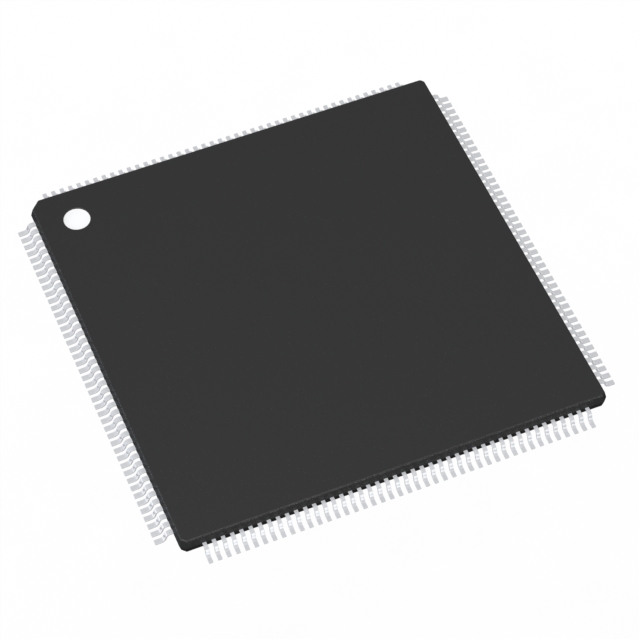
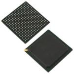
In the pursuit of higher reliability, reduced board space, and improved electrical performance, the integration of passive components directly into the circuit board structure represents a significant advancement. The Buried Resistor Capacitor PCB technology embeds resistive and capacitive elements within the inner layers of the board, eliminating surface-mounted passive components and delivering measurable improvements in signal integrity, assembly efficiency, and long-term reliability. HONTEC has established itself as a trusted manufacturer of Buried Resistor Capacitor PCB solutions, serving high-tech industries across 28 countries with specialized expertise in high-mix, low-volume, and quick-turn prototype production.
The value of Buried Resistor Capacitor PCB construction extends beyond simple component consolidation. By embedding passive elements into the board structure, this technology eliminates thousands of solder joints that would otherwise be potential failure points in complex assemblies. Signal paths are shortened, parasitic inductance is reduced, and board real estate previously consumed by discrete components becomes available for active devices or design simplification. Applications ranging from high-speed digital systems and RF modules to medical implants and aerospace electronics increasingly rely on Buried Resistor Capacitor PCB technology to meet aggressive size, weight, and performance targets.
Located in Shenzhen, Guangdong, HONTEC combines advanced manufacturing capabilities with rigorous quality standards. Every Buried Resistor Capacitor PCB produced carries the assurance of UL, SGS, and ISO9001 certifications, while the company actively implements ISO14001 and TS16949 standards. With logistics partnerships that include UPS, DHL, and world-class freight forwarders, HONTEC ensures efficient global delivery. Every inquiry receives a response within 24 hours, reflecting a commitment to responsiveness that global engineering teams value.
The advantages of Buried Resistor Capacitor PCB technology over discrete surface-mount passive components span multiple dimensions of product development and manufacturing. Reliability represents one of the most significant benefits, as each embedded passive element eliminates two solder joints that would otherwise exist with a discrete component. For boards utilizing hundreds or thousands of resistors and capacitors, this reduction in solder joints dramatically decreases the statistical probability of assembly-related failures. Electrical performance improves substantially with embedded passives. The elimination of component leads and solder joints reduces parasitic inductance and capacitance, enabling cleaner power distribution and improved signal integrity at high frequencies. Space savings on the board surface allow designers to reduce overall board size or utilize the freed area for additional functionality. Assembly costs decrease as the number of components requiring placement and inspection declines, while inventory management simplifies with fewer part numbers to track. HONTEC works with clients to evaluate design requirements against the benefits of embedded passives, identifying applications where the technology delivers maximum return on investment. For high-volume applications with consistent passive requirements, the Buried Resistor Capacitor PCB approach often proves more cost-effective than discrete alternatives when total system costs are considered.
Achieving precise electrical values in Buried Resistor Capacitor PCB fabrication requires specialized materials and process controls that differ significantly from standard PCB manufacturing. For embedded resistors, HONTEC utilizes resistive foil materials with controlled sheet resistivity, typically available in values ranging from 10 to 1000 ohms per square. The resistance value of each buried resistor is determined by the geometry of the resistive element—specifically the length-to-width ratio of the pattern defined during fabrication. Laser trimming systems provide fine adjustment of resistance values after initial fabrication, allowing HONTEC to achieve tolerances as tight as ±1% for critical applications. For embedded capacitors, dielectric materials with specific thickness and dielectric constant values are used to create capacitive structures between copper planes. The capacitance value is determined by the area of the overlapping plates, the dielectric thickness, and the material’s dielectric constant. HONTEC utilizes precision layer registration and controlled lamination processes to maintain consistent dielectric thickness across the board, ensuring uniform capacitance values. Both resistor and capacitor structures are verified through electrical testing after fabrication, with test coupons integrated into the production panel providing verification of passive component values before final board processing. This combination of precision fabrication and verification ensures that Buried Resistor Capacitor PCB products meet the electrical specifications required for demanding applications.
Implementing Buried Resistor Capacitor PCB technology successfully requires design considerations that extend beyond conventional PCB layout practices. HONTEC engineering team emphasizes early collaboration as the most critical factor, as embedded passive structures influence layer stack-up, material selection, and manufacturing process flow. Designers must specify which resistors and capacitors will be embedded, as not all passive components are suitable candidates. Values that remain consistent across production volumes are ideal for embedding, while values requiring frequent design changes are better implemented as discrete components. The layout of embedded passives requires attention to the interface between embedded elements and connecting circuitry, with via placement and trace routing designed to minimize parasitic effects. Thermal management considerations become relevant for embedded resistors that dissipate significant power, as heat must be conducted through surrounding dielectric materials. HONTEC provides design guidelines covering minimum resistor dimensions, recommended geometries for different resistance values, and spacing requirements between embedded elements and other board features. The engineering team also assists with stack-up optimization, ensuring that embedded passives are positioned within the board structure to balance electrical performance with manufacturability. By addressing these considerations during design, clients achieve Buried Resistor Capacitor PCB solutions that maximize the benefits of passive integration while maintaining predictable manufacturing outcomes.
HONTEC maintains manufacturing capabilities spanning the full range of Buried Resistor Capacitor PCB requirements. Resistor values from 10 ohms to 1 megohm are supported with tolerances down to ±1% where critical applications demand. Capacitor values from a few picofarads to several nanofarads per square inch are achievable through standard dielectric materials, with expanded ranges available for specialized applications.
Layer counts for Buried Resistor Capacitor PCB construction range from simple 2-layer designs with embedded resistors to complex multilayer structures incorporating both embedded resistors and capacitors across multiple layers. Material selections include standard FR-4 for general applications, high-Tg materials for enhanced thermal stability, and low-loss laminates for high-frequency designs where embedded passives contribute to signal integrity.
For engineering teams seeking a manufacturing partner capable of delivering reliable Buried Resistor Capacitor PCB solutions from prototype through production, HONTEC offers technical expertise, responsive communication, and proven quality systems backed by international certifications.

MC24M Buried capacitance PCB--Ordinary chip capacitors are placed on empty PCBs through SMT; buried capacitance is to integrate new buried capacitance materials into PCB / FPC, which can save PCB space and reduce EMI / noise suppression, etc. Currently answering MEMS microphones And communications have been widely used.The following is about MC24M Buried Capacitor PCB related, I hope to help you better understand MC24M Buried Capacitor PCB.

24-Layer Buried capacitance PCB has a process called burying resistance, which is to put chip resistors and chip capacitors into the inner layer of the PCB board. These chip resistors and capacitors are generally very small, such as 0201, or even smaller 01005. The PCB board produced in this way is the same as a normal PCB board, but a lot of resistors and capacitors are placed in it. For the top layer, the bottom layer saves a lot of space for component placement. The following is about 24 Layer Buried capacitance PCB related, I hope to help you better understand 24 Layer Buried capacitance PCB.