In applications where circuit boards face repeated insertion, harsh environments, or critical contact reliability, the surface finish becomes a defining factor in product longevity. The Hard gold PCB provides the exceptional wear resistance, corrosion protection, and consistent contact performance required for high-reliability interconnections. HONTEC has established itself as a trusted manufacturer of Hard gold PCB solutions, serving high-tech industries across 28 countries with specialized expertise in high-mix, low-volume, and quick-turn prototype production.
Hard gold plating differs fundamentally from soft gold or immersion gold finishes commonly used in PCB manufacturing. By incorporating hardening agents such as cobalt or nickel into the gold deposit, Hard gold PCB construction creates a surface that withstands thousands of insertion cycles without degradation. Applications ranging from edge connectors and backplanes to military electronics and industrial control systems depend on Hard gold PCB technology to maintain electrical integrity over decades of service.
Located in Shenzhen, Guangdong, HONTEC combines advanced manufacturing capabilities with rigorous quality standards. Every Hard gold PCB produced carries the assurance of UL, SGS, and ISO9001 certifications, while the company actively implements ISO14001 and TS16949 standards. With logistics partnerships that include UPS, DHL, and world-class freight forwarders, HONTEC ensures efficient global delivery. Every inquiry receives a response within 24 hours, reflecting a commitment to responsiveness that global engineering teams value.
The distinction between Hard gold PCB and other gold finishes lies in the composition, thickness, and intended application of the gold deposit. ENIG, or electroless nickel immersion gold, applies a thin layer of gold—typically 0.05 to 0.1 microns—over a nickel barrier. This finish provides excellent solderability and surface flatness for fine-pitch component assembly but offers minimal wear resistance. Soft gold, or pure gold plating, provides good corrosion protection but lacks the hardness to withstand repeated mechanical contact. A Hard gold PCB utilizes gold alloyed with hardening agents, typically cobalt or nickel, deposited at significantly greater thickness—ranging from 0.5 to 2.0 microns or more. This combination of alloy composition and thickness creates a surface with hardness values typically exceeding 130 HK (Knoop hardness), compared to 30 to 60 HK for soft gold. The resulting Hard gold PCB surface withstands the mechanical abrasion of repeated connector insertion and extraction without exposing the underlying nickel or copper. Additionally, hard gold provides superior corrosion resistance in harsh environments, maintaining low and stable contact resistance across the product lifespan. HONTEC works with clients to determine appropriate gold thickness and hardness specifications based on expected insertion cycles, environmental exposure, and contact force requirements.
Achieving consistent gold thickness and reliable adhesion in Hard gold PCB fabrication requires specialized plating processes and rigorous quality controls. HONTEC employs electrolytic gold plating systems designed specifically for hard gold deposition, with precisely controlled current density, solution chemistry, and plating time to achieve uniform thickness across the board surface. The process begins with proper surface preparation, including cleaning, micro-etching, and activation steps that ensure the underlying nickel or copper surface is free from contamination and receptive to gold deposition. HONTEC applies a nickel underplate beneath the hard gold layer, typically 3 to 5 microns thick, which serves as a diffusion barrier preventing copper migration to the gold surface and providing mechanical support for the gold deposit. The nickel layer also contributes to overall contact hardness and corrosion resistance. Plating thickness is monitored through X-ray fluorescence measurement systems that verify gold and nickel thickness at multiple points across each Hard gold PCB. Adhesion testing, including tape testing and thermal shock evaluation, confirms that the plated layers remain securely bonded under stress. HONTEC maintains process controls that ensure gold thickness remains within specified tolerances, typically ±20% of target, across all plated features. This systematic approach ensures that Hard gold PCB products deliver the wear resistance and contact reliability expected for demanding applications.
Hard gold PCB technology is specified for applications where electrical contacts are subject to repeated mechanical engagement or harsh environmental exposure. Edge connectors and card-edge interfaces represent the most common application, where boards are inserted and removed from sockets or mating connectors multiple times during product assembly, testing, and field service. HONTEC recommends Hard gold PCB construction for any design requiring more than 25 insertion cycles, with gold thickness scaled according to expected cycle count. Backplanes for telecommunications and server infrastructure utilize hard gold on connector fingers and mating interfaces to ensure signal integrity across years of operation. Military and aerospace electronics specify Hard gold PCB construction for its proven reliability under vibration, temperature extremes, and corrosive atmospheric conditions. Industrial control systems, including programmable logic controllers and motor drives, depend on hard gold contacts for consistent performance in factory environments. HONTEC advises clients on design considerations specific to hard gold fabrication, including gold finger beveling for smooth insertion, contact spacing and positioning relative to board edges, and the use of solder mask dams to prevent solder wicking onto gold fingers during assembly. The engineering team also provides guidance on the interface between hard gold areas and other board finishes, ensuring that adjacent ENIG or HASL areas do not compromise hard gold performance. By addressing these considerations during design, clients achieve Hard gold PCB solutions that deliver reliable connections throughout the product lifecycle.
HONTEC maintains manufacturing capabilities spanning the full range of Hard gold PCB requirements. Gold thickness from 0.5 microns to 2.0 microns is supported, with hardness levels appropriate to application wear requirements. Selective plating capabilities allow hard gold to be applied only to contact areas, reducing material costs while maintaining performance where needed.
Board constructions incorporating Hard gold PCB technology range from simple 2-layer designs to complex multilayer boards with high-density routing. HONTEC supports both tab plating for edge connectors and selective plating for internal contact features. Beveling services ensure smooth insertion of gold fingers into mating connectors.
For engineering teams seeking a manufacturing partner capable of delivering reliable Hard gold PCB solutions from prototype through production, HONTEC offers technical expertise, responsive communication, and proven quality systems backed by international certifications.

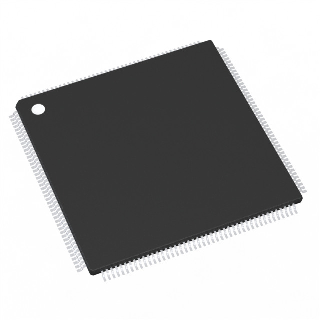
The golden finger is composed of many golden yellow conductive contacts. It is called "golden finger" because its surface is gilded and the conductive contacts are arranged like fingers. The step gold finger PCB is actually coated with a layer of gold on the copper clad laminate by a special process, because the gold has strong oxidation resistance and strong conductivity.

The EM-530K PCB is actually coated with a layer of gold on the copper clad laminate by a special process, because the gold has strong oxidation resistance and strong conductivity.

Hard gold PCB--plating gold can be divided into hard gold and soft gold. Because the hard gold plating is an alloy, the hardness is relatively hard. It is suitable for use in places where friction is required. It is generally used as a contact point on the edge of the PCB (commonly known as gold fingers).The following is about Hard gold plated PCB related, I hope to help you better understand Hard gold plated PCB.

Gold finger PCB In the extensive use of PCI cable socket gold fingers, gold fingers have been divided into: long and short gold fingers, broken gold fingers, split gold fingers, and gold finger boards. In the process of processing, gold-plated wires need to be pulled. Comparison of conventional gold finger processing processes Simple, long and short gold fingers, the need to strictly control the lead of the gold fingers, requires a second etching to complete.The following is about Gold finger Board related, I hope to help you better understand Gold finger Board.