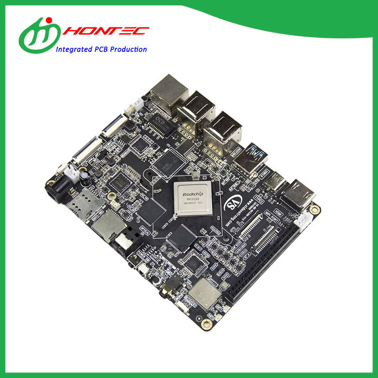
In the journey from bare circuit board to finished electronic product, the assembly phase represents the critical transition where design becomes reality. PCBA, or printed circuit board assembly, encompasses the full process of component placement, soldering, inspection, and testing that transforms a bare board into a functional electronic module. HONTEC has established itself as a trusted provider of PCBA solutions, serving high-tech industries across 28 countries with specialized expertise in high-mix, low-volume, and quick-turn prototype assembly.
The value of a comprehensive PCBA service extends far beyond simple component attachment. From sourcing authentic components and managing supply chain logistics to implementing assembly processes optimized for specific board types and delivering fully tested assemblies ready for system integration, HONTEC provides end-to-end solutions that simplify the production process. Applications ranging from medical devices and industrial controls to telecommunications equipment and automotive electronics benefit from PCBA capabilities that combine technical expertise with operational efficiency.
Located in Shenzhen, Guangdong, HONTEC operates with certifications including UL, SGS, and ISO9001, while actively implementing ISO14001 and TS16949 standards. The company partners with UPS, DHL, and world-class freight forwarders to ensure efficient global delivery of finished assemblies. Every inquiry receives a response within 24 hours, reflecting a commitment to responsiveness that global engineering teams value.
The PCBA process at HONTEC encompasses a comprehensive sequence of operations designed to deliver fully functional electronic assemblies. The process begins with component procurement, where HONTEC sources authentic components from authorized distributors and verified supply chains, managing bill of materials verification and inventory coordination. Solder paste application utilizes stencil printing systems with controlled deposition to ensure consistent solder volume across all pads. Component placement employs high-speed pick-and-place equipment capable of handling components ranging from 01005 passives to large ball grid array packages, with vision systems verifying placement accuracy. Reflow soldering utilizes precisely profiled thermal cycles tailored to each assembly’s thermal mass and component sensitivity, ensuring complete solder joint formation without component damage. For assemblies requiring both surface mount and through-hole components, selective soldering or wave soldering processes are applied. HONTEC implements automated optical inspection at critical stages, verifying solder joint quality, component orientation, and placement accuracy. X-ray inspection is utilized for ball grid array and other hidden-joint components to confirm solder ball collapse and void levels. Functional testing, in-circuit testing, and boundary scan testing validate that the PCBA meets electrical specifications before shipment. This comprehensive approach ensures that each PCBA arrives ready for system integration.
Ensuring PCBA reliability for complex or high-reliability applications requires quality control measures that extend beyond standard manufacturing practices. HONTEC implements a multi-layered quality management system specifically designed for critical assemblies. Solder paste inspection verifies volume, area, and height of paste deposits before component placement, preventing defects related to insufficient or excessive solder. Automated optical inspection after placement confirms component position and orientation before reflow, allowing correction before soldering occurs. Post-reflow inspection utilizes both 2D and 3D optical systems that detect solder bridging, insufficient wetting, tombstoning, and other common defects. For PCBA designs with fine-pitch components or ball grid array packages, X-ray inspection provides visibility of hidden solder joints, verifying ball collapse, void content, and alignment. Process control systems track reflow oven parameters including temperature profile, conveyor speed, and atmosphere, ensuring consistent thermal exposure across every assembly. HONTEC implements cleanliness testing for PCBA products destined for high-reliability applications, verifying that flux residues and contaminants are removed to specified levels. Environmental stress screening, including thermal cycling and vibration testing, is available for applications requiring validated reliability. Traceability systems link each PCBA to its manufacturing data, component lots, and test results, supporting quality analysis and field failure investigation. This layered approach to quality control ensures that PCBA products meet the reliability expectations of demanding applications.
Design for manufacturability considerations play a crucial role in achieving successful PCBA outcomes, and HONTEC provides early engineering engagement to identify optimization opportunities. Component selection influences assembly yield, with HONTEC advising on package types that balance functionality with manufacturability. Fine-pitch components require precise solder paste stencil design and accurate placement; where design flexibility allows, slightly larger package options can improve assembly margins. Pad geometry and solder mask definitions directly affect solder joint formation, with HONTEC providing guidance on land pattern dimensions that balance reliability with manufacturability. Thermal management during assembly requires consideration of component placement relative to large thermal masses; HONTEC advises on placement strategies that minimize temperature gradients during reflow. Panelization and breakaway tab design influence handling and depaneling processes, with HONTEC providing recommendations that balance assembly efficiency with board integrity. Test point accessibility affects in-circuit testing capability; HONTEC reviews test point placement to ensure access within test fixture constraints. For PCBA designs incorporating both surface mount and through-hole components, HONTEC evaluates assembly sequence and thermal profiles to ensure all solder joints meet quality standards. By addressing these considerations during design, clients achieve PCBA outcomes that balance functionality, manufacturability, and cost.
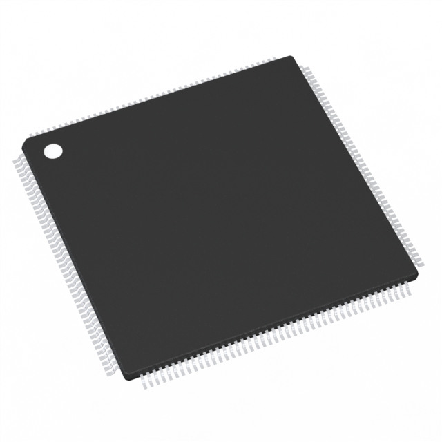
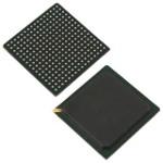
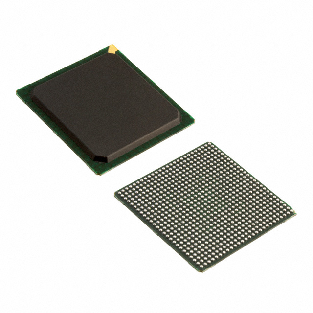
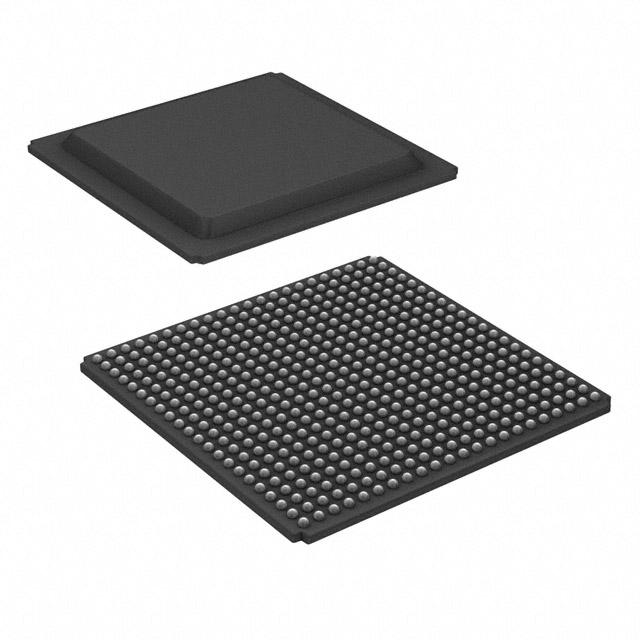
HONTEC maintains assembly capabilities spanning the full range of PCBA requirements. Surface mount technology supports component sizes from 01005 to large ball grid arrays, with placement accuracy suitable for fine-pitch applications. Through-hole assembly capabilities accommodate both manual and selective soldering processes for mixed-technology designs.
Component sourcing extends to authentic components from leading manufacturers worldwide, with HONTEC managing supply chain verification, inventory coordination, and obsolescence management. Testing capabilities include in-circuit testing, flying probe testing, functional testing, and boundary scan testing, with custom test fixture development available for production programs.
For engineering teams seeking a manufacturing partner capable of delivering reliable PCBA solutions from prototype through production, HONTEC offers technical expertise, responsive communication, and proven quality systems backed by international certifications.

HONTEC has 30 medical PCBA production lines such as Panasonic and Yamaha, Germany ersa selective wave soldering, solder paste detection 3D SPI, AOI, X-ray, BGA repair table and other equipment.

We provide a full range of electronic manufacturing services, from PCBA to OEM / ODM, including design support, procurement, SMT, testing and assembly. If we choose HONTEC, our customers will enjoy an extremely flexible one-stop processing and manufacturing service.

HONTEC is a professional PCB assembly one-stop service provider, PCB design, component procurement, PCB manufacturing, SMT processing, assembly, etc

Communication PCBA is the abbreviation of printed circuit board + assembly, that is to say, PCBA is the whole process of PCB SMT, then dip plug-in.

Industrial control PCBA generally refers to a processing flow, which can also be understood as the finished circuit board, that is, PCBA can only be counted after the processes on the PCB are completed. PCB refers to an empty printed circuit board with no parts on it.