As electronic systems grow increasingly sophisticated, the demand for higher component density, improved signal integrity, and enhanced thermal management continues to rise. The Multilayer PCB has become the standard for applications ranging from telecommunications infrastructure and medical devices to automotive electronics and industrial control systems. HONTEC has established itself as a trusted manufacturer of Multilayer PCB solutions, serving high-tech industries across 28 countries with specialized expertise in high-mix, low-volume, and quick-turn prototype production.
The value of a Multilayer PCB lies in its ability to accommodate complex routing requirements within a compact footprint. By stacking multiple conductive layers separated by insulating materials, these boards provide dedicated power planes, ground planes, and signal layers that work together to maintain signal integrity while minimizing electromagnetic interference. HONTEC combines advanced manufacturing capabilities with rigorous quality standards to deliver Multilayer PCB products that meet the most demanding specifications.
Located in Shenzhen, Guangdong, HONTEC operates with certifications including UL, SGS, and ISO9001, while actively implementing ISO14001 and TS16949 standards. The company partners with UPS, DHL, and world-class freight forwarders to ensure efficient global delivery. Every inquiry receives a response within 24 hours, reflecting a commitment to responsiveness that global engineering teams value.
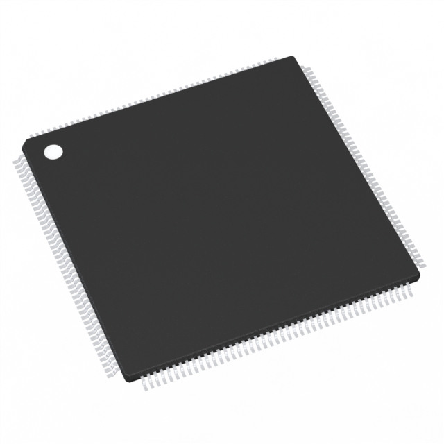
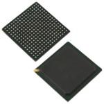
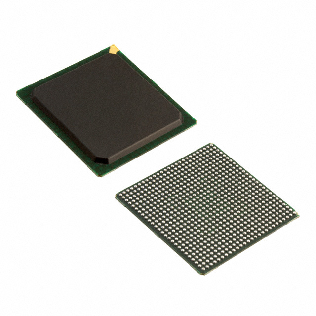
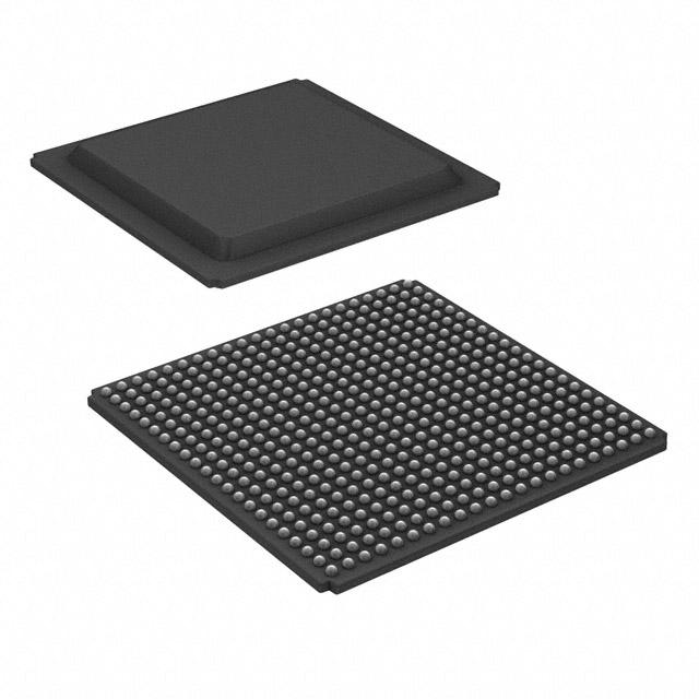
The layer count of a Multilayer PCB directly influences both electrical performance and manufacturing cost. Additional layers provide dedicated routing channels that reduce signal congestion and allow for clean separation between analog, digital, and power circuits. For high-speed designs, dedicated ground planes adjacent to signal layers create controlled impedance transmission lines that maintain signal integrity across the board. However, each added layer increases material costs, extends fabrication time, and adds complexity to lamination and registration processes. HONTEC recommends determining layer count based on specific design requirements rather than arbitrary targets. A 4-layer Multilayer PCB often provides sufficient routing density for many applications while offering significant performance advantages over 2-layer designs through dedicated power and ground planes. As component density increases or signal speeds rise, 6-layer or 8-layer configurations become necessary. For designs with extremely high pin-count components or complex routing requirements, HONTEC supports layer counts up to 20 layers with sequential lamination techniques that maintain registration accuracy. The engineering team assists clients in optimizing layer stack-ups to achieve the required performance without unnecessary cost.
Reliability in Multilayer PCB manufacturing demands rigorous quality control at every stage of production. HONTEC implements comprehensive inspection and testing protocols designed specifically for multilayer construction. Automated optical inspection verifies inner layer patterns before lamination, ensuring that any defects are caught before layers become inaccessible. X-ray inspection confirms layer registration after lamination, detecting any misalignment that could compromise interlayer connections. Impedance testing validates that controlled impedance traces meet design specifications, using time-domain reflectometry to measure characteristic impedance across critical nets. Cross-section analysis provides visual confirmation of plating thickness, layer alignment, and via integrity, with samples taken from each production batch. Electrical testing verifies continuity and isolation for every net, ensuring that no opens or shorts exist in the completed Multilayer PCB. Thermal stress testing simulates assembly conditions, subjecting boards to multiple reflow cycles to identify any latent defects such as delamination or barrel cracks. HONTEC maintains traceability records that link each Multilayer PCB to its manufacturing parameters, supporting quality analysis and continuous improvement efforts.
Material selection fundamentally shapes the electrical, thermal, and mechanical performance of any Multilayer PCB. Standard FR-4 materials provide a cost-effective solution for many applications, offering adequate thermal stability and dielectric properties for general-purpose designs. For Multilayer PCB applications requiring enhanced thermal performance, high-Tg materials maintain mechanical stability under elevated temperatures encountered during assembly and operation. High-speed digital designs demand low-loss materials such as Isola FR408 or Panasonic Megtron series, which minimize signal attenuation and maintain consistent dielectric constant across frequency ranges. RF and microwave applications require specialized laminates from Rogers or Taconic that deliver stable electrical properties at high frequencies. HONTEC works with clients to select materials that align with specific application requirements, considering factors such as operating frequency, temperature range, and environmental exposure. Mixed dielectric constructions combine different material types within a single Multilayer PCB, optimizing performance for critical signal layers while maintaining cost efficiency for non-critical layers. The engineering team provides guidance on material compatibility, ensuring that the selected laminates bond properly during lamination and maintain reliability throughout the product lifecycle.
HONTEC maintains manufacturing capabilities spanning the full range of Multilayer PCB requirements. Standard multilayer production accommodates 4 to 20 layers with conventional through-hole vias and advanced registration systems that maintain alignment across the entire stack. For designs requiring higher density, HDI capabilities support blind vias, buried vias, and microvia structures that enable finer routing geometries and reduced board size.
Copper weights from 0.5 oz to 4 oz accommodate diverse current-carrying requirements, while surface finish options include HASL, ENIG, immersion silver, and immersion tin to match assembly processes and environmental requirements. HONTEC processes both prototype and production quantities with lead times optimized for engineering validation and volume manufacturing.
For engineering teams seeking a manufacturing partner capable of delivering reliable Multilayer PCB solutions, HONTEC offers technical expertise, responsive communication, and proven quality systems backed by international certifications.

ST115G PCB -- with the development of integrated technology and microelectronic packaging technology, the total power density of electronic components is growing, while the physical size of electronic components and electronic equipment is gradually tending to be small and miniaturized, resulting in rapid accumulation of heat, resulting in the increase of heat flux around the integrated devices. Therefore, high temperature environment will affect the electronic components and devices This requires a more efficient thermal control scheme. Therefore, the heat dissipation of electronic components has become a major focus in the current electronic components and electronic equipment manufacturing.

Halogen-free PCB -- halogen (halogen) is a group VII a non-gold Duzhi element in Bai, including five elements: fluorine, chlorine, bromine, iodine and astatine. Astatine is a radioactive element, and the halogen is usually referred to as fluorine, chlorine, bromine and iodine. Halogen-free PCB is environmental protection PCB does not contain the above elements.

Tg250 PCB is made of polyimide material. It can withstand high temperature for a long time and does not deform at 230 degrees. It is suitable for high temperature equipment, and its price is slightly higher than that of ordinary FR4

S1000-2M PCB is made of S1000-2M material with TG value of 180. It is a good choice for Multilayer PCB with high reliability, high cost performance, high performance, stability and practicality

For high-speed applications, the performance of plate plays an important role. IT180A PCB belongs to high Tg board, which is also commonly used high Tg board. It has high cost performance, stable performance, and can be used for signals within 10G.

ENEPIG PCB is the abbreviation of gold plating, palladium plating and nickel plating. ENEPIG PCB coating is the latest technology used in electronic circuit industry and semiconductor industry. The gold coating with thickness of 10 nm and palladium coating with thickness of 50 nm can achieve good conductivity, corrosion resistance and friction resistance.