Optoelectronic PCB is a core component in modern optical and electronic integration, supporting applications where light-based signals and electronic control must operate with precision and stability. This article provides a comprehensive explanation of how optoelectronic PCB works, the challenges customers face during design and manufacturing, and how to select reliable solutions for demanding environments. It also explains material choices, structural design considerations, quality control methods, and application scenarios, helping engineers and decision-makers reduce risk and improve system performance. HONTEC delivers optoelectronic PCB solutions designed for reliability, scalability, and long-term operational stability.
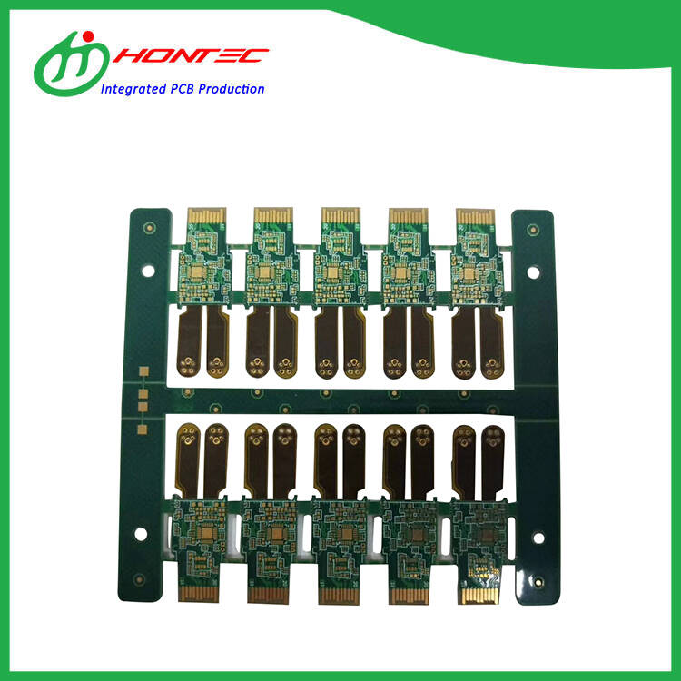
An optoelectronic PCB is a printed circuit board engineered to integrate optical components, such as LEDs, photodiodes, laser devices, or optical sensors, with electronic circuits. Unlike conventional PCBs, optoelectronic PCBs must manage both electrical signal integrity and optical performance, often within compact and thermally demanding environments.
These boards are widely used in communication systems, industrial sensing, automotive electronics, medical devices, and advanced consumer products. HONTEC focuses on optoelectronic PCB designs that ensure stable signal transmission, precise optical alignment, and consistent thermal performance.
Customers working with optoelectronic PCB often face complex challenges that directly affect product reliability and time to market.
These pain points highlight the importance of integrated design, controlled manufacturing processes, and experienced technical support.
An optoelectronic PCB typically consists of multiple functional layers, each designed to support specific performance requirements.
Proper integration of these elements ensures both optical accuracy and electrical reliability throughout the product lifecycle.
Material selection plays a decisive role in optoelectronic PCB performance. The wrong material can compromise optical clarity, thermal stability, or long-term reliability.
HONTEC evaluates material performance based on operating environment, optical requirements, and expected service life to deliver optimized solutions.
Successful optoelectronic PCB design requires close coordination between optical, electrical, and mechanical considerations.
A well-planned design reduces rework, improves yield, and ensures stable optical output in real-world conditions.
Manufacturing optoelectronic PCB demands strict process control to maintain consistency and accuracy.
HONTEC applies standardized production procedures and continuous monitoring to ensure every optoelectronic PCB meets design specifications.
| PCB Type | Key Features | Primary Advantages | Typical Uses |
|---|---|---|---|
| Standard PCB | Electrical-only design | Low cost | Basic electronics |
| High-Speed PCB | Controlled impedance | Signal stability | Data communication |
| Optoelectronic PCB | Optical and electrical integration | Precision and reliability | Optical sensing and transmission |
Optoelectronic PCB solutions support a wide range of advanced applications.
Reliability testing is essential to verify optoelectronic PCB performance under real operating conditions.
HONTEC implements multi-stage inspection and testing to ensure consistent quality and dependable performance.
What makes optoelectronic PCB different from standard PCB?
Optoelectronic PCB integrates optical components and requires precise alignment, thermal control, and material selection beyond standard electrical designs.
Can optoelectronic PCB be customized?
Yes. Layout, materials, and layer structures can be customized based on optical and electrical requirements.
How is heat managed in optoelectronic PCB?
Thermal vias, high-conductivity substrates, and optimized layouts are commonly used to dissipate heat.
Is optoelectronic PCB suitable for mass production?
With proper design and process control, optoelectronic PCB supports both low-volume prototypes and large-scale manufacturing.
Optoelectronic PCB is a critical foundation for modern systems that rely on accurate light-based signal transmission and electronic control. By addressing design complexity, material selection, and manufacturing precision, businesses can achieve higher reliability and better long-term performance.
HONTEC provides professional optoelectronic PCB solutions tailored to complex application requirements. If you are planning a new optical system or looking to improve existing designs, contact us to discuss your technical needs and discover how HONTEC can support your project with stable, high-quality optoelectronic PCB manufacturing.