

Summary: Heavy copper PCBs are essential for high-power, high-reliability applications. This article explores their benefits, design considerations, manufacturing processes, and practical applications to help engineers and businesses optimize electronic performance while reducing failures.
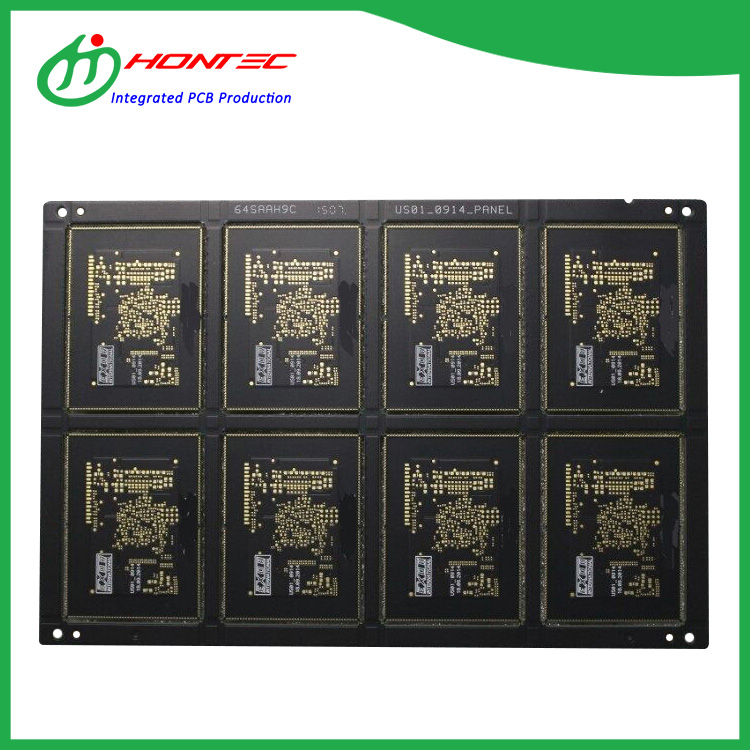
Table of Contents
What is Heavy Copper PCB?
Heavy copper PCBs are printed circuit boards designed with copper thicknesses exceeding standard levels, typically 3oz/ft² (105 μm) or more. They handle higher currents, dissipate heat efficiently, and are essential for industrial power electronics, automotive electronics, and high-current circuits.
Compared to standard PCBs, heavy copper PCBs provide:
- Enhanced current-carrying capacity
- Improved thermal management
- Increased mechanical strength
- Longer service life under demanding conditions
Advantages of Heavy Copper PCB
| Feature | Benefit |
|---|---|
| High Current Capacity | Supports higher amperage without excessive heating. |
| Excellent Heat Dissipation | Reduces risk of component failure due to thermal stress. |
| Mechanical Strength | Resists warping and deformation during operation. |
| Durability | Extends PCB lifespan in harsh industrial environments. |
These benefits make heavy copper PCBs indispensable in sectors where reliability and performance are non-negotiable.
Design Considerations for Heavy Copper PCBs
Designing heavy copper PCBs requires careful attention to factors that affect performance and manufacturability:
- Trace Width and Thickness: Ensure traces handle the required current without overheating.
- Thermal Management: Use thermal vias, planes, and heat sinks to dissipate heat efficiently.
- Material Selection: Choose substrates like FR-4, polyimide, or metal-core boards based on thermal and mechanical needs.
- Plating Techniques: Electrodeposited copper ensures uniform thickness and reliability.
- Panelization: Optimize for manufacturing yield and reduce waste.
Heavy Copper PCB Manufacturing Process
The production of heavy copper PCBs involves several critical steps:
- Base Material Preparation: Selection of high-quality substrate and pre-bond copper foils.
- Lamination: Pressing copper layers and prepreg under high heat and pressure.
- Patterning: Using photolithography to define circuit paths.
- Etching: Removing excess copper to leave desired traces.
- Electroplating: Building up additional copper for high-current traces.
- Surface Finishing: Applying HASL, ENIG, or other finishes for solderability.
- Testing: Electrical, thermal, and mechanical testing to ensure performance standards.
Applications of Heavy Copper PCBs
Heavy copper PCBs are widely used in industries where durability and high-power handling are critical:
- Industrial power supplies and inverters
- Electric vehicles and charging stations
- Telecom and 5G infrastructure
- Medical imaging and high-power diagnostic equipment
- High-current LED lighting systems
Maintenance Tips for Heavy Copper PCBs
Proper care ensures longevity and reliable operation:
- Regular visual inspection for corrosion, delamination, or overheating.
- Check solder joints for cracks and reinforce if necessary.
- Clean with non-abrasive, anti-static solutions.
- Ensure proper thermal management during operation.
- Follow manufacturer guidelines for electrical load limits.
Frequently Asked Questions
- Q1: Can heavy copper PCBs handle extremely high currents?
- Yes, with proper trace design and copper thickness, they can handle currents above 100A depending on the application.
- Q2: How thick can the copper layer be?
- Typical heavy copper PCBs range from 3oz (105 μm) to 10oz (350 μm) per layer.
- Q3: Are heavy copper PCBs more expensive?
- They are generally costlier than standard PCBs due to additional materials and manufacturing complexity, but their performance and longevity justify the investment.
- Q4: Which industries benefit most from heavy copper PCBs?
- Industries like automotive, industrial power, aerospace, medical devices, and telecom benefit significantly from their high current and thermal performance.
Contact HONTEC
HONTEC specializes in high-quality heavy copper PCBs that meet demanding industrial and commercial standards. Our expertise ensures reliable, high-performance circuit boards for your most critical applications. For more details and customized solutions, contact us today.