Article Summary
High-speed PCB plays a critical role in modern electronic products where data rates, signal integrity, and system stability are essential. From communication equipment and servers to automotive electronics and industrial control systems, High-speed PCB design directly affects performance and reliability. This article provides a comprehensive explanation of High-speed PCB fundamentals, design considerations, material selection, and practical parameters, helping readers understand how High-speed PCB solves real-world engineering challenges.

Outline
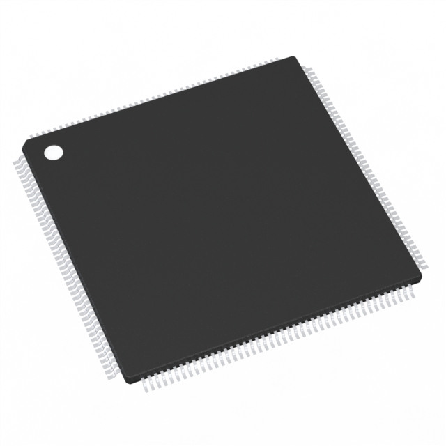
High-speed PCB refers to printed circuit boards designed to handle high-frequency and high-speed digital signals with minimal distortion and loss. As signal rise times become shorter and data rates increase, traditional PCB design methods are no longer sufficient. High-speed PCB focuses on controlling impedance, minimizing crosstalk, reducing electromagnetic interference, and maintaining signal integrity across the entire transmission path.
Rather than simply routing traces between components, High-speed PCB design treats each signal path as a controlled transmission line. This shift in design philosophy is essential for meeting the performance demands of modern electronic systems.
Modern electronic systems operate at increasingly higher speeds. Interfaces such as PCIe, USB, HDMI, Ethernet, and high-speed memory all rely on precise signal timing and waveform integrity. Without High-speed PCB design techniques, systems may experience data errors, signal reflection, excessive noise, or complete functional failure.
High-speed PCB addresses customer pain points such as unstable communication, excessive electromagnetic radiation, reduced product lifespan, and difficulty passing compliance testing. By integrating electrical, material, and manufacturing considerations, High-speed PCB ensures reliable operation even under demanding conditions.
Several fundamental principles guide High-speed PCB design. These principles work together to maintain signal quality throughout the circuit.
These principles are applied throughout schematic design, layout planning, and manufacturing preparation to ensure consistency from concept to finished product.
Material selection is a decisive factor in High-speed PCB performance. Dielectric constant stability, dissipation factor, and thermal behavior all influence signal transmission quality.
Common material categories used in High-speed PCB include advanced FR-4, low-loss laminates, and high-frequency materials. The choice depends on operating frequency, signal rise time, and environmental requirements.
Stack-up strategy determines how signal layers, power planes, and ground planes are arranged. A well-designed stack-up reduces impedance variation, suppresses noise coupling, and simplifies manufacturing control.
| Parameter | Description |
|---|---|
| Operating Frequency | Defines the maximum signal frequency the PCB can reliably support |
| Dielectric Constant | Impacts signal propagation speed and impedance stability |
| Dissipation Factor | Indicates signal energy loss during transmission |
| Impedance Tolerance | Controls reflection and signal distortion |
| Layer Count | Supports signal isolation, power integrity, and routing density |
| Copper Thickness | Affects resistance, heat dissipation, and impedance calculation |
High-speed PCB design introduces challenges that differ from conventional PCB development. Common issues include signal reflection, crosstalk between adjacent traces, power integrity problems, and electromagnetic interference.
Solutions involve precise impedance modeling, controlled spacing between traces, optimized power distribution networks, and proper use of stitching vias and reference planes. Advanced simulation and validation methods further reduce design risk before manufacturing.
High-speed PCB technology is widely applied across multiple industries. Typical application areas include data centers, telecommunications infrastructure, automotive electronics, medical equipment, and industrial automation.
In these scenarios, system reliability and long-term stability are critical. High-speed PCB ensures that complex electronic systems operate consistently under high data throughput and challenging environmental conditions.
What differentiates High-speed PCB from standard PCB?
High-speed PCB focuses on transmission line behavior, impedance control, and signal integrity, while standard PCB primarily addresses basic connectivity and electrical functionality.
Does High-speed PCB require special manufacturing processes?
Yes, tighter tolerances, controlled dielectric materials, and precise layer alignment are often required to meet High-speed PCB performance targets.
How does High-speed PCB improve system reliability?
By minimizing signal distortion, reducing noise, and stabilizing power distribution, High-speed PCB ensures consistent performance and reduces failure risk in high-speed systems.
High-speed PCB is a foundational technology for advanced electronic systems that demand accuracy, speed, and stability. Through careful design, material selection, and manufacturing control, High-speed PCB enables reliable high-frequency signal transmission across diverse applications.
With extensive experience in High-speed PCB development and manufacturing, HONTEC delivers solutions tailored to complex technical requirements and real-world operating conditions. For customized High-speed PCB solutions that support your next-generation electronic products, contact us today to discuss your project needs and technical goals.