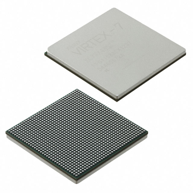
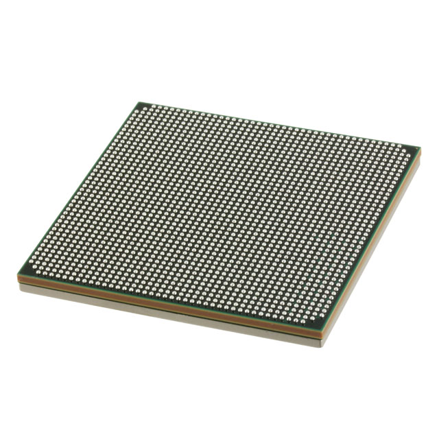
Chip is the general term of semiconductor component products. Chip is also called integrated circuit and IC. What material is the chip mainly composed of? Let's have a look!

Cutting, fillet, edging, baking, inner layer pretreatment, coating, exposure, DES (development, etching, film removal), punching, AOI inspection, VRS repair, browning, lamination, pressing, target drilling, Gong edge, drilling, copper plating, film pressing, printing, writing, surface treatment, final inspection, packaging and other processes are countless

People who make circuit boards know that the production process is very complex~

the difference between longitude and latitude causes the change of substrate size; Due to the failure to pay attention to the fiber direction during shearing, the shear stress remains in the substrate.

The development of printed circuit board substrate materials has gone through nearly 50 years

Integrated circuit is a way of miniaturization of circuits (mainly including semiconductor equipment, also including passive components, etc.). Using a certain process, the transistors, resistors, capacitors, inductors and other components and wiring required in a circuit are interconnected, fabricated on a small or several small semiconductor chips or dielectric substrates,