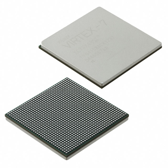
Faced with the increasingly high integration of hardware platforms and more and more complex electronic systems, the PCB layout should have a modular thinking, which requires the use of modularity in the design of hardware schematics and PCB wiring. , Structured design method. As a hardware engineer, on the premise of understanding the overall architecture of the system, first of all, we should consciously merge modular design ideas in the schematic diagram and PCB wiring design, combined with the actual situation of the PCB, plan the basic idea of PCB layout.
Here is a function of arranging components, that is, arranging in a rectangular area, which can combine the interaction of components in the early stage of the layout to conveniently separate a bunch of messy components according to modules and place them in a certain area.
(1) Select all the components of one of the modules on the schematic, then the components on the PCB corresponding to the schematic are selected.
(2) Execute the menu command "Tools-Device placement-Arrange in rectangular area".
(3) Select a range in a blank area on the PCB. At this time, the components of this functional module will be arranged within the range of this frame selection. Using this function, you can quickly divide all the functional modules on the schematic.
Modular layout and interactive layout are inseparable. Use the interactive layout to select all the components of the module on the schematic and arrange them one by one on the PCB. Next, you can further refine the layout of ICs, resistors, and diodes. This is the PCB modular layout.