HDI imaging, while achieving low defect rate and high output, can achieve stable production of HDI conventional high-precision operation. For example: advanced mobile phone board, CSP pitch is less than 0.5mm. The board structure is 3 + n + 3, there are three superposed vias on each side, and 6 to 8 layers of coreless printed boards with superimposed vias.The following is about Medical Equipment PCB related, I hope to help you better understand Medical Equipment PCB.

VT-870 PCB refers to the HDI circuit board with more than 2 levels, usually 3 + N + 3 or 4 + N + 4 or 5 + N + 5 structure. The blind hole uses a laser, and the hole copper is about 15UM.The following is about 18 layer 3step HDI circuit board related, I hope to help you better understand 18 layer 3step HDI circuit board.

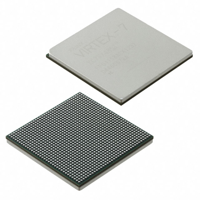
HDI is the English abbreviation of High Density Interconnector, high-density interconnect (HDI) manufacturing printed circuit board. The printed circuit board is a structural element formed by insulating material supplemented by conductor wiring. The following is about 10 Layer 4Step HDI PCB related, I hope to help you better understand 10 Layer 4Step HDI PCB.

24Layers ELIC PCB--When a printed circuit board is made into a final product, integrated circuits, transistors (triodes, diodes), passive components (such as resistors, capacitors, connectors, etc.) and various other electronic parts are mounted on it. The following is about 24 Layers of Any Connected HDI related, I hope to help you better understand 24 Layers of Any Connected HDI.

R-5735 PCB--Any hole with a diameter of less than 150um is called microvia in the industry, and the circuit made by this geometric technology of microvia can improve the benefits of assembly, space utilization, etc. At the same time, it also has the effect of miniaturization of electronic products. Its necessity. The following is about Matte Black HDI Circuit Board related, I hope to help you better understand Matte Black HDI Circuit Board.

HDI boards are generally manufactured using a lamination method. The more laminations, the higher the technical level of the board. Ordinary HDI boards are basically laminated one time. High-level HDI adopts two or more layered technologies. At the same time, advanced PCB technologies such as stacked holes, electroplated holes, and direct laser drilling are used. The following is about 8 Layer Robot HDI PCB related, I hope to help you better understand Robot HDI PCB.