In the landscape of modern electronics, circuit density and signal integrity define the boundary between a functional device and a market-leading innovation. As electronic systems grow more compact while demanding higher performance, the Multilayer Board has emerged as the foundational technology that enables this evolution. HONTEC stands at the forefront of this domain, delivering high-mix, low-volume, and quick-turn prototype Multilayer Board solutions to high-tech industries across 28 countries.
The complexity of a Multilayer Board extends far beyond simply adding more layers. Each additional layer introduces considerations of impedance control, thermal management, and interlayer registration that demand precision manufacturing capabilities. HONTEC operates from a strategic location in Shenzhen, Guangdong, where advanced fabrication facilities meet rigorous quality standards. Every Multilayer Board produced carries the assurance of UL, SGS, and ISO9001 certifications, with ongoing implementation of ISO14001 and TS16949 standards that reflect a commitment to environmental responsibility and automotive-grade quality systems.
For engineers designing for telecommunications, medical devices, aerospace systems, or industrial controls, the choice of a Multilayer Board manufacturer directly impacts time-to-market and product reliability. HONTEC combines technical expertise with responsive service, partnering with UPS, DHL, and world-class freight forwarders to ensure that prototype and production orders reach destinations worldwide without delay. Every inquiry receives a response within 24 hours, reflecting a customer-first approach that has built lasting partnerships across the globe.
Determining the appropriate layer count for a Multilayer Board requires balancing electrical performance, physical space constraints, and manufacturing complexity. The primary considerations begin with signal routing requirements. High-speed digital designs often demand dedicated layers for power planes and ground planes to maintain signal integrity and reduce electromagnetic interference. When component density increases, additional signal layers become necessary to accommodate routing without violating spacing rules. Thermal management also influences layer count, as additional copper planes can serve as heat spreaders for power-intensive components. HONTEC typically recommends that clients evaluate the number of critical nets requiring controlled impedance, the availability of board real estate, and the desired aspect ratio for via structures. A well-planned Multilayer Board with appropriate layer count reduces the need for costly redesigns during prototype validation and ensures that the final product meets both electrical and mechanical requirements.
Layer-to-layer registration is one of the most critical quality parameters in Multilayer Board fabrication. HONTEC employs advanced optical alignment systems and multi-stage registration controls throughout the manufacturing process. The process begins with precision drilling of registration holes in each individual layer using laser-guided systems that achieve positional accuracy within microns. During the lamination phase, specialized pin lamination systems ensure that all layers remain perfectly aligned under high temperature and pressure. After lamination, X-ray inspection systems verify registration accuracy before proceeding to subsequent processes. For Multilayer Board designs exceeding twelve layers or incorporating sequential lamination techniques, HONTEC utilizes automated optical inspection at multiple stages to detect any misalignment before it compromises the final product. This rigorous approach to registration ensures that buried vias, blind vias, and interlayer connections maintain electrical continuity across the entire stack, preventing open circuits or intermittent failures that could arise from layer shifting.
Reliability testing for a Multilayer Board encompasses both electrical verification and physical stress assessment. HONTEC implements a comprehensive testing protocol that begins with electrical testing using flying probe or fixture-based systems to verify continuity and isolation for every net. For Multilayer Board designs with high-density interconnect features, impedance testing is performed using time-domain reflectometry to ensure characteristic impedance meets specified tolerances. Thermal stress testing subjects the boards to multiple cycles of extreme temperature variations to identify any latent defects such as barrel cracks or delamination. Additional tests include ionic contamination analysis to verify cleanliness, solder float testing for surface finish integrity, and micro-sectioning analysis that allows internal inspection of via structures and layer bonds. HONTEC maintains detailed traceability records for each Multilayer Board, enabling clients to access quality documentation and test results. This multi-layered approach to testing ensures that boards perform reliably in their intended application environments, whether subjected to automotive thermal cycling, industrial vibration, or long-term operational demands.
The distinction between a standard supplier and a trusted manufacturing partner becomes evident when design challenges arise. HONTEC provides engineering support that extends from design for manufacturability reviews to material selection guidance for Multilayer Board projects. Clients benefit from access to technical expertise that helps optimize layer stack-ups, reduce fabrication costs, and anticipate potential manufacturing constraints before they impact schedules.
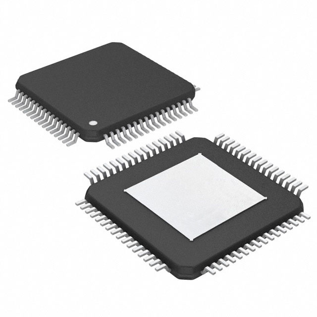
The Multilayer Board fabrication capabilities at HONTEC span from 4-layer prototypes to complex 20-layer structures incorporating blind vias, buried vias, and controlled impedance profiles. Material selection options include standard FR-4 for cost-sensitive applications, high-performance materials like Megtron and Isola for high-frequency requirements, and specialized laminates for RF and microwave applications.
With a responsive team committed to clear communication and a logistics network built for global reach, HONTEC delivers Multilayer Board solutions that align technical excellence with operational efficiency. For design engineers and procurement professionals seeking a reliable partner for complex PCB requirements, HONTEC represents a proven choice backed by certifications, experience, and a customer-first philosophy.

ST115G PCB -- with the development of integrated technology and microelectronic packaging technology, the total power density of electronic components is growing, while the physical size of electronic components and electronic equipment is gradually tending to be small and miniaturized, resulting in rapid accumulation of heat, resulting in the increase of heat flux around the integrated devices. Therefore, high temperature environment will affect the electronic components and devices This requires a more efficient thermal control scheme. Therefore, the heat dissipation of electronic components has become a major focus in the current electronic components and electronic equipment manufacturing.

Halogen-free PCB -- halogen (halogen) is a group VII a non-gold Duzhi element in Bai, including five elements: fluorine, chlorine, bromine, iodine and astatine. Astatine is a radioactive element, and the halogen is usually referred to as fluorine, chlorine, bromine and iodine. Halogen-free PCB is environmental protection PCB does not contain the above elements.

Tg250 PCB is made of polyimide material. It can withstand high temperature for a long time and does not deform at 230 degrees. It is suitable for high temperature equipment, and its price is slightly higher than that of ordinary FR4

S1000-2M PCB is made of S1000-2M material with TG value of 180. It is a good choice for Multilayer PCB with high reliability, high cost performance, high performance, stability and practicality

For high-speed applications, the performance of plate plays an important role. IT180A PCB belongs to high Tg board, which is also commonly used high Tg board. It has high cost performance, stable performance, and can be used for signals within 10G.

ENEPIG PCB is the abbreviation of gold plating, palladium plating and nickel plating. ENEPIG PCB coating is the latest technology used in electronic circuit industry and semiconductor industry. The gold coating with thickness of 10 nm and palladium coating with thickness of 50 nm can achieve good conductivity, corrosion resistance and friction resistance.