Multilayer PCB technology has become the backbone of advanced electronic manufacturing. From industrial automation systems to telecommunications equipment and medical devices, multilayer printed circuit boards enable compact layouts, faster signal transmission, and higher reliability. This article explains how multilayer PCBs work, their advantages, manufacturing challenges, material options, and how choosing the right PCB manufacturer like HONTEC can improve product quality and long-term performance.
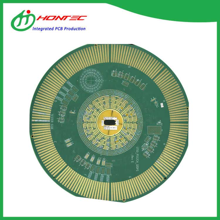
A multilayer PCB is a printed circuit board composed of three or more conductive copper layers laminated together with insulating materials. Unlike single-sided or double-sided PCBs, multilayer boards allow engineers to create more complex and compact electronic circuits within limited space.
Modern electronic devices demand higher speed, better signal integrity, and reduced electromagnetic interference. Multilayer PCB structures solve these problems by distributing power planes, ground planes, and signal layers efficiently.
| PCB Type | Number of Layers | Complexity | Typical Use |
|---|---|---|---|
| Single-Sided PCB | 1 | Low | Simple electronics |
| Double-Sided PCB | 2 | Medium | Industrial controls |
| Multilayer PCB | 3+ Layers | High | Servers, telecom, medical devices |
A multilayer PCB works by stacking conductive and insulating layers together into one compact structure. Copper traces on each layer carry electrical signals between components, while vias connect the internal layers vertically.
The internal design usually includes:
This layered structure significantly improves signal integrity and reduces electromagnetic interference. High-speed electronic systems such as 5G communication devices and AI servers rely heavily on multilayer PCB architecture to maintain stable operation.
Multilayer PCB technology provides several advantages compared with traditional PCB structures.
More circuits can be integrated into a smaller footprint, enabling compact consumer electronics and portable devices.
Internal connections are protected within the board structure, reducing external damage and improving durability.
Dedicated ground and power planes minimize signal distortion and electromagnetic interference.
Thermal distribution across multiple layers improves device stability and operating lifespan.
Multilayer PCBs are widely used across industries requiring high-density circuitry and reliable performance.
| Industry | Application |
|---|---|
| Telecommunications | 5G base stations, routers, signal processors |
| Medical | Imaging systems, monitoring equipment |
| Automotive | ADAS systems, battery management |
| Industrial Automation | Robotics, PLC controllers |
| Consumer Electronics | Smartphones, laptops, gaming devices |
As devices become smaller and more powerful, the demand for multilayer PCB manufacturing continues to increase globally.
Material selection directly impacts electrical performance, thermal stability, and product lifespan.
For high-speed communication systems, low-loss materials are critical to maintain stable signal transmission and reduce insertion loss.
Manufacturing multilayer PCB boards requires strict process control and advanced fabrication equipment.
Precision during layer alignment is essential because even minor deviations may affect signal performance and reliability.
Manufacturers such as HONTEC focus on advanced multilayer PCB fabrication technologies, including impedance control, HDI structures, buried vias, and high-frequency PCB solutions to meet modern industrial requirements.
Despite its advantages, multilayer PCB design introduces several technical challenges.
To avoid costly redesigns, engineers should collaborate closely with PCB manufacturers during the early design stage. Proper stack-up planning and DFM analysis help improve manufacturability and reduce production risk.
Selecting the right PCB manufacturing partner directly affects product quality, lead time, and long-term reliability.
When evaluating a multilayer PCB supplier, consider the following factors:
HONTEC provides professional multilayer PCB manufacturing services for industries requiring precision, consistency, and advanced technology support. Their capabilities include high-layer-count boards, HDI PCB fabrication, and high-frequency PCB production for demanding applications.
A double-sided PCB contains two conductive layers, while a multilayer PCB contains three or more layers stacked together for higher circuit density and performance.
They improve signal integrity, reduce noise, and provide stable power distribution, which is essential for high-speed electronic systems.
Yes. Due to advanced manufacturing processes, additional materials, and strict quality requirements, multilayer PCBs generally cost more than standard PCB types.
Telecommunications, automotive electronics, medical equipment, aerospace, and industrial automation industries heavily depend on multilayer PCB technology.
Looking for a reliable multilayer PCB manufacturer with advanced production capabilities and strict quality control?
HONTEC provides professional multilayer PCB solutions for telecommunications, industrial electronics, automotive systems, medical equipment, and high-frequency applications.
Whether you need prototype development or large-volume PCB production, our engineering team is ready to support your project requirements with fast response and dependable manufacturing services.
Please contact us today for technical consultation and customized multilayer PCB solutions.