Manufacturing process of printed circuit board
1、 Overview
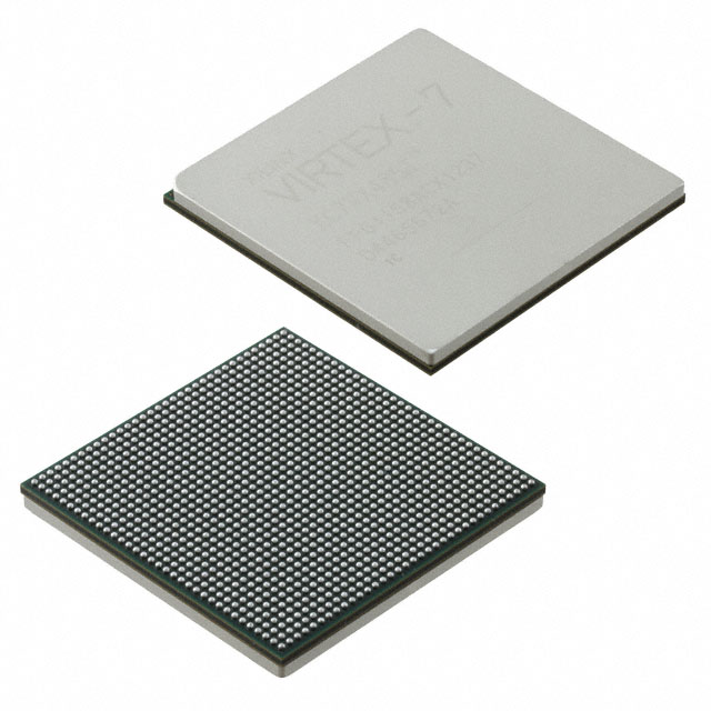
PCB, the abbreviation of printedcircuit board, is translated into printed circuit board in Chinese. It includes single-sided, double-sided and multilayer printed boards with rigidity, flexibility and rigidity torsion combination.
PCB is an Zui important basic component of electronic products, which is used as the interconnection and mounting substrate of electronic components. Different types of PCBs have different manufacturing processes, but the basic principles and methods are roughly the same, such as electroplating, etching, resistance welding and other process methods. Among all kinds of PCBs, rigid multilayer PCB is widely used Zui, and its manufacturing process method and process Zui are representative, which is also the basis of other types of PCB manufacturing processes. Understanding the manufacturing process method and process of PCB and mastering the basic manufacturing process ability of PCB are the basis of PCB manufacturability design. In this article, we will briefly introduce the manufacturing methods, processes and basic process capabilities of traditional rigid multilayer PCB and high-density interconnect PCB.
2、 Rigid multilayer PCB
Rigid multilayer PCB is the PCB used in most electronic products at present. Its manufacturing process is representative, and it is also the process basis of HDI board, flexible board and rigid flex combination board.
technological process:
The manufacturing process of rigid multilayer PCB can be simply divided into four stages: inner laminate manufacturing, lamination / lamination, drilling / electroplating / outer circuit manufacturing, resistance welding / surface treatment.
Stage 1: manufacturing process method and flow of inner plate
Stage 2: lamination / lamination process method and process
Stage 3: drilling / electroplating / outer circuit manufacturing process method and process
Stage 4: resistance welding / surface treatment process method and process
3、 With the use of BGA and BTC components with lead center distance of 0.8mm and below, the traditional manufacturing process of laminated printed circuit can not meet the application needs of micro spacing components, so the manufacturing technology of high-density interconnect (HDI) circuit board is developed.
The so-called HDI board generally refers to PCB with line width / line distance less than or equal to 0.10mm and micro conduction aperture less than or equal to 0.15mm.
In the traditional multilayer board process, all layers are stacked into a PCB at one time, and the through through holes are used for interlayer connection. In the HDI board process, the conductor layer and the insulating layer are stacked layer by layer, and the conductors are connected through micro buried / blind holes. Therefore, HDI board process is generally called build-up process (BUP, build-up process or bum, build-up music player). According to the method of micro buried / blind hole conduction, it can also be further subdivided into electroplated hole deposition process and applied conductive paste deposition process (such as ALIVH process and b2it process).
1. Structure of HDI board
The typical structure of HDI board is "n + C + n", where "n" represents the number of lamination layers and "C" represents the core board. With the increase of interconnection density, full stack structure (also known as arbitrary layer interconnection) has also been used.
2. Electroplating hole process
In the process of HDI board, electroplated hole process is the mainstream, accounting for almost more than 95% of the HDI board market. It is also developing. From the early traditional hole electroplating to hole filling electroplating, the design freedom of HDI board has been greatly improved.
3. ALIVH process this process is a multi-layer PCB manufacturing process with full build-up structure developed by Panasonic. It is a build-up process using conductive adhesive, which is called any layer interstitial viahole (ALIVH), which means that any inter layer interconnection of the build-up layer is realized by buried / blind through holes.
The core of the process is hole filling with conductive adhesive.
ALIVH process features:
1) Using non-woven aramid fiber epoxy resin semi cured sheet as substrate;
2) The through hole is formed by CO2 laser and filled with conductive paste.
4. B2it process
This process is the manufacturing process of laminated multilayer board, which is called buried bump interconnection technology (b2it). The core of the process is the bump made of conductive paste.