DHI board surface treatment technology carbon series direct plating
1.History of carbon series direct plating
The carbon series direct plating process has been widely used in the circuit board industry for 35 years. Processes widely used in industry include black holes, eclipses, and shadows. The original black hole direct plating technology was patented in 1984 and has been commercially successful as a plating FR-4 through-hole panel process.
Because the black hole is a coating process, not a redox process like chemical copper sink, the technology is not sensitive to the surface activity of different dielectric materials and can handle materials that are difficult to metallize. Therefore, this process has been widely used in polyimide films in flexible circuits, high-performance or special materials, such as polytetrafluoroethylene (PTFE). The direct plating technology of carbon and graphite is approved for aerospace and military avionics applications and meets the requirements of section 3.2.6.1 of the IPC-6012D specification.
2.Circuit board development
With the need for printed circuit board design, direct electroplating processes have continued to develop in the past few years. Due to the miniaturization drive, from lead components to surface mount components, PCB design has evolved to adapt to micro components with more pins, which results in increased PCB layers, thicker circuit boards, and through holes The diameter is smaller. In order to meet the challenges of high aspect ratio, the technical specifications of the production line should involve the improvement of the solution transfer and exchange of micropores, such as the use of ultrasonic waves to quickly wet the pores and remove air bubbles, and the ability to improve the air knife and dryer to effectively dry thick circuits. Small holes on the board.
Since then, PCB designers have entered the next stage: blind hole hunger, the number of pins and the density of the ball grid exceed the board surface available for drilling and wiring. With the 1.27mm to 1.00mm grid of ball grid array packages (BGA) and the 0.80mm to 0.64mm grid of chip scale packages (CSP), micro blind holes have become a weapon for designers to meet the challenges of HDI technology.
In 1997, feature phones began to use the 1 + N+1 design for mass production; this is a design with micro-blind holes in the overlay on the layer core. With the growth of mobile phone sales, pre-etching windows and CO2 lasers , UV, UV-YAG laser and combined UV-CO2 laser to form micro blind holes. Micro-blind vias allow designers to route under the blind vias, so they can redistribute more pin grids without increasing the number of layers. HDI is currently widely used in three platforms: miniaturized products, high-end packaging and high-performance electronic products. Miniaturization in mobile phone design is currently the most productive application.
3.Direct plating
Direct plating systems such as black holes must overcome technical obstacles to meet the metallization challenges of blind holes and HDI microvias. When the size of the blind hole is reduced, the difficulty of removing carbon particles at the bottom of the blind hole is increased, but the cleanliness of the bottom of the blind hole is a key factor that affects reliability; therefore, the development of new cleaners and micro-etching agents is to improve blindness How to clean the bottom of the hole.
In addition, based on theory and practical experience, the nozzle design of the micro-erosion section was modified to be a combination of spraying-soaking-spraying configuration. Practice has proved to be an effective design. The distance between the nozzle and the surface of the circuit board is reduced, the distance between the nozzles is reduced, and the spray impact force on the circuit board is increased. By grasping the details, the new nozzle design can effectively handle high aspect ratio through holes and blind holes.
With the development of the next generation of smart phones, manufacturers began to use any layer of stacked blind hole design to eliminate through holes, which triggered a trend that as the line width and line spacing were reduced from 60μm to 40μm, the production of circuit boards The original copper foil thickness used in the process is steadily reduced from 18 μm to 12 μm to 9 μm. And each superimposed layer of any layer circuit board needs to be metallized and electroplated once, which greatly increases the capacity demand of the wet process.
smartphones are also the main users of flexible and rigid-flex circuits. Compared with the traditional chemical copper plating process, the application of direct plating in the production of any layer, flexible circuit board (FPC) and rigid-flex circuit board has increased significantly, because this process is compared with the traditional chemical copper process Lower cost, less water usage, less waste water production
4.PCB's increasingly narrow line width/line spacing requirements require strict control of etching depth
Now, the latest generation of smartphones and advanced packaging are gradually adopting the alternative semi-additive method (mSAP). mSAP uses 3μm ultra-thin foil to achieve 30/30 micron line width and pitch design. In the production process using ultra-thin copper foil, it is necessary to precisely control the amount of bite corrosion of micro-etching grooves in each process. Especially for traditional chemical copper immersion and direct plating processes, the amount of bite corrosion of the surface copper foil must be controlled very accurately
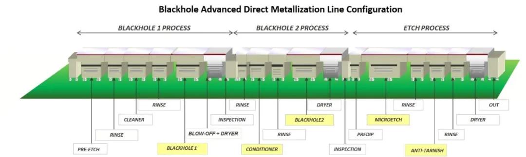
5.Advances in equipment configuration
In order to optimize the direct plating process to match the mSAP process, several different equipment designs were gradually tested on the experimental line before being put into full production. The test results show that, through good equipment design, a uniform conductive carbon coating can be provided under a wide operating range.
For example, in the direct plating process of the carbon series, a patented roller configuration is used to make the carbon coating more uniform. And reduce the amount of carbon deposition on the surface of the production board, reduce the amount of carbon suspension, and at the same time prevent the excessively thick carbon layer at the corners of blind holes or through holes.
The equipment specifications of the post-microetching tank have also been redesigned. Whether the bottom of the blind hole is 100% completely clean is the manufacturer's most concerned quality issue. If there is carbon residue at the bottom of the blind hole, it can pass the test during the electrical test, but because the cross-sectional area of the conduction is reduced, the bonding force is also reduced, resulting in breakage due to the absence of thermal stress during assembly The problem of failure. As the diameter of the blind hole is reduced from the traditional 100 microns to 150 microns to 80 microns to 60 microns, upgrading the equipment specifications of the micro-etching groove is critical to product reliability.
Through testing and research to modify the equipment specifications of the micro-etching tank to improve the process capability to completely remove the carbon residue at the bottom of the blind hole, it has been applied to mass production lines. The first major improvement includes the use of dual etch grooves to provide more precise control of the amount of bite. In the first stage, most of the carbon on the copper surface is removed, and in the second stage, fresh and clean micro-etching solution is used to prevent the carbon particles from returning to the mass production board. In the second stage, the technology of reducing copper wire was also adopted to greatly improve the uniformity of the micro-etching on the surface of the circuit board.
Reducing the variability of the amount of bite on the circuit board surface helps to accurately control the total etching amount at the bottom of the blind hole. The variability of the amount of bite is strictly controlled by the chemical concentration, nozzle design and spray pressure parameters
6.Chemical improvement
In terms of chemical improvement, the traditional pore cleaning agents and micro-etching potions were tested and modified, while considering the ability to control bite corrosion. The organic additives in the cleaning agent are selectively deposited only on the copper surface, and will not be deposited on the resin material. Therefore, carbon particles will only be deposited on this special organic coating. When the circuit board enters the micro-etching groove, the organic coating has high solubility in the acidic liquid. Therefore, the organic coating is removed by the acid in the micro-etching groove, and at the same time, the copper surface under the carbon particles is side-etched, which can accelerate Remove carbon particles on the same side.
Another improvement project is that the use of two-component micro-etching can improve the ability to remove carbon particles and reduce the micro-roughness of the copper foil surface. Let the roughness of the copper surface be conducive to dry film adhesion. The test results show that the relatively smooth bottom of the blind hole helps to improve the reliability of the plating at the bottom of the blind hole. After the optimized carbon series direct plating process, the copper foil at the bottom of the blind hole has been completely clean, which can allow the electroplated copper to continue to grow on the copper lattice on the copper foil to achieve the best plating adhesion.
The combination of key process tanks and specific improvements in chemicals constitute an advanced HDI/mSAP process suitable for production using ultra-thin copper foil. Through a single interface of copper-copper direct bonding, a continuous metal lattice is formed, which improves the reliability of blind holes. The treatment of the micro-etching groove allows the ideal micro-roughness of the copper foil at the bottom of the blind hole to be used as a hole-filling electroplated copper substrate. This promotes the continuous growth of the lattice of electroplated copper on the bottom of the blind hole along the lattice of the copper foil. After the normal high-temperature heat treatment, the copper grains are arranged in a lattice and form a complete continuous metal lattice.
Observation and analysis of FIB cutting samples to form thin slices show that the interface lines are uniform in grain size and structure (Figure 5). After thermal shock or thermal cycling, the boundary between the copper foil at the bottom of the blind hole and the electroplated copper is difficult It is found that there is no Nano-void that other processes are prone to, unless it is caused by factors such as oxidation or pollution.
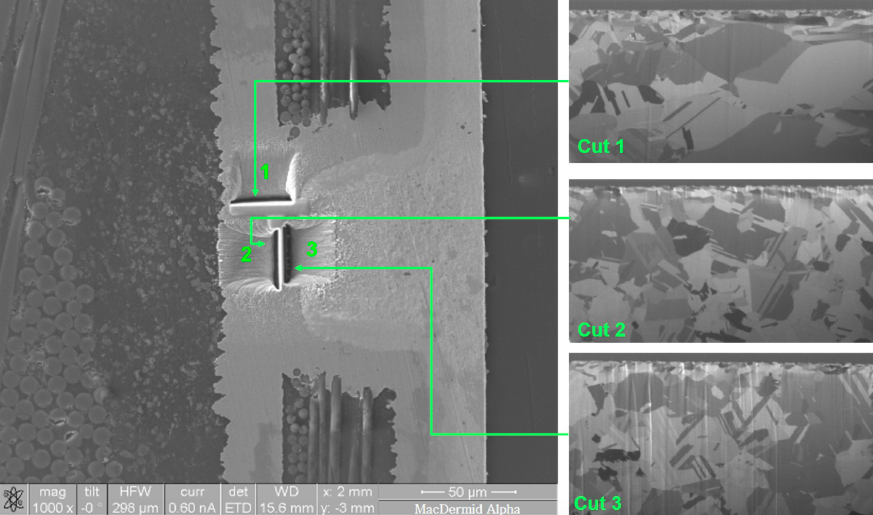
Focused ion beam (FIB) imaging of the interface between the electroplated copper layer and the target pad, leading direct electroplating technology enables strong copper-copper bonding to perform well under thermal stress.
Direct electroplating production lines, such as "black holes", are currently used in the mass production process of alternative semi-additive (mSAP) of 3 micron ultra-thin copper foil. These systems use related equipment that precisely controls the amount of micro-etching in mass production. The 12-layer circuit board produced with this equipment has passed the 300 Cycle IST test. In the above products, black holes are used in L2/10 and L3/11 using the mSAP process. The size of the blind holes is 80~100 x 45μm, and each circuit board contains 2 million blind holes.
Use AOI to check for carbon residues in the process. The inspection results showed that in the 5,000 PSM/month output, no defects were detected. The electroplating of these circuit boards is done on a vertical continuous electroplating (VCP) production line; the inner layer adopts the full-plate electroplating of the Tent-Etch process, and the mSAP layer must be pattern electroplating. The electron backscatter diffraction (EBSD) image in Figure 6 shows the uniformity of the grain size at the interface between the target pad and the electroplated copper layer.