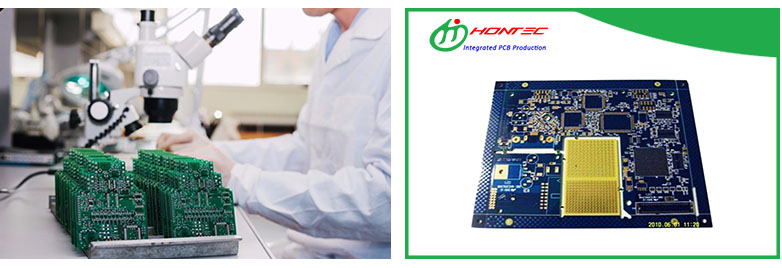
Buried vias: Buried vias only connect the traces between the inner layers, so they are not visible from the PCB surface. Such as 8layer board, the holes of 2-7 layers are buried holes.The following is about Mechanical Blind Buried Hole PCB related, I hope to help you better understand Mechanical Blind Buried Hole PCB.
Quick Details of Blind Buried Hole PCB
Place of Origin: Guangdong, China
Brand Name: Medical device PCB Model Number: Rigid-PCB
Base Material: EMC EM-526
Copper Thickness: 1oz Board Thickness: 2mm
Min. Hole Size: 0.2mm Min. Line Width: 4mil Min. Line Spacing: 4mil
Surface Finishing: ENIG and Hard gold
Number of layers: 10L PCB Standard: IPC-A-600
Solder Mask: Blue
Legend: White
Product quotation: Within 2 Hours
Service: 24Hours technical services Sample delivery: Within 8 days

HONTEC Quick Electronics Limited (HONTEC), established in 2009, is one of leading quickturn Printed Circuit Board manufacturer, who specializes in high-mix, low volume and quickturn prototype PCB for high-tech industries in 28 countries. Upon efficiently quick around operation, PCB products contain 4 to 48 layers, HDI, Heavy Copper, Rigid-Flex, high frequency microwave,and Embedded Capacitance, and provides "PCB One-stop Shop" service to meet customers’ diverse demands. HONTEC is capable of producing 4,500 varieties monthly to meet 24-hour delivery for 4 layers PCB, 48-hour for 6 layers and 72-hour for 8 or more high-layer PCB at the fastest. Located in SiHui of GuangDong,HONTEC partners up with UPS, DHL and world-class forwarders to provide efficient shipping services.