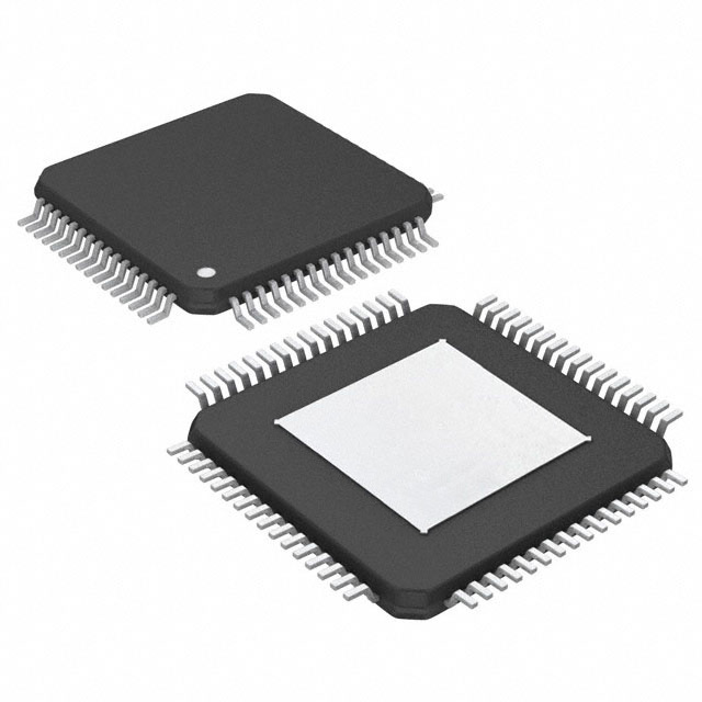
In the vast landscape of electronic design, the Double-sided PCB occupies a unique position—offering the complexity to support sophisticated circuitry while maintaining the cost-effectiveness and straightforward manufacturing that make it accessible for countless applications. HONTEC has established itself as a trusted manufacturer of Double-sided PCB solutions, serving high-tech industries across 28 countries with specialized expertise in high-mix, low-volume, and quick-turn prototype production.
The Double-sided PCB provides the ideal balance for designs that require more routing capacity than single-sided boards can offer but do not demand the layer count and complexity of multilayer constructions. By placing copper traces on both sides of the substrate and connecting them through plated through-holes, this construction doubles the available routing area while maintaining a simple, reliable manufacturing process. Applications ranging from power supplies and industrial controls to consumer electronics and automotive systems depend on Double-sided PCB technology to deliver consistent performance at predictable cost points.
Located in Shenzhen, Guangdong, HONTEC combines advanced manufacturing capabilities with rigorous quality standards. Every Double-sided PCB produced carries the assurance of UL, SGS, and ISO9001 certifications, while the company actively implements ISO14001 and TS16949 standards. With logistics partnerships that include UPS, DHL, and world-class freight forwarders, HONTEC ensures efficient global delivery. Every inquiry receives a response within 24 hours, reflecting a commitment to responsiveness that global engineering teams value.
The choice between a Double-sided PCB and other constructions depends on the specific requirements of the application. Single-sided boards place copper traces on only one surface, limiting routing options and typically requiring jumper wires for circuits that must cross. A Double-sided PCB adds copper on both sides, connected by plated through-holes that allow traces to transition between layers. This doubles the available routing area and eliminates the need for jumpers, enabling more compact designs and cleaner layouts. Multilayer boards add additional internal layers, offering even higher density but at increased cost and longer lead times. HONTEC recommends a Double-sided PCB for designs with moderate component counts, mixed analog and digital sections that benefit from separate ground planes, or applications where cost efficiency is a primary consideration. For designs requiring more than two signal layers or complex impedance control, multilayer construction becomes necessary. The engineering team at HONTEC provides guidance during the design review phase, helping clients evaluate factors such as component density, signal integrity requirements, and production volume to determine the optimal construction for their specific application.
Plated through-holes represent the critical interconnection feature in any Double-sided PCB, as they provide the electrical pathway between top and bottom layers while also serving as mechanical anchors for component leads. HONTEC implements a comprehensive process control system to ensure through-hole reliability. The process begins with precision drilling using carbide bits that maintain hole diameter tolerances within ±0.05mm. Following drilling, a desmear process removes any debris and prepares the hole walls for copper deposition. Electroless copper plating creates a thin conductive layer across the hole walls, followed by electrolytic copper plating that builds up to the specified thickness, typically 0.025mm or greater. HONTEC conducts destructive cross-section analysis on every production batch, allowing visual inspection of copper thickness distribution, plating uniformity, and interface integrity. Thermal stress testing simulates assembly conditions by subjecting the Double-sided PCB to multiple reflow cycles, with continuity testing performed between cycles to detect any via cracking or separation. For designs with particularly high reliability requirements, HONTEC offers enhanced plating processes and additional testing protocols. This systematic approach to through-hole quality ensures that the Double-sided PCB maintains electrical continuity and mechanical integrity throughout its operational life.
HONTEC employs a multi-stage testing protocol to verify that every Double-sided PCB meets design specifications before shipment. Electrical testing forms the foundation of quality verification, utilizing flying probe or fixture-based test systems to confirm continuity for every net and isolation between adjacent nets. For Double-sided PCB designs with impedance-critical traces, time-domain reflectometry testing verifies that characteristic impedance falls within specified tolerances. Automated optical inspection scans the entire board surface to detect defects such as shorts, opens, insufficient solder mask coverage, or trace irregularities that might escape electrical testing. Visual inspection under magnification confirms that silkscreen markings are legible, surface finish is uniform, and overall workmanship meets HONTEC quality standards. For each production batch, documentation includes a certificate of conformance detailing the testing performed and results. Additional documentation available includes material certificates verifying laminate provenance, impedance test reports for controlled impedance designs, and cross-section images showing plating quality. HONTEC maintains traceability records that allow individual Double-sided PCB units to be tracked through the manufacturing process, providing clients with confidence in quality and supporting any necessary field analysis. This comprehensive testing and documentation approach ensures that boards arrive ready for assembly with minimal risk of manufacturing-related defects.
HONTEC maintains manufacturing capabilities spanning the full range of Double-sided PCB requirements. Material options include standard FR-4 for general applications, high-Tg materials for designs requiring enhanced thermal stability, and aluminum-backed substrates for LED lighting and power applications requiring improved heat dissipation.
Copper weights from 0.5 oz to 4 oz accommodate everything from fine-pitch signal routing to high-current power distribution. Surface finish selections include HASL for cost-sensitive applications, ENIG for designs requiring flat surfaces for fine-pitch components, and immersion silver for applications where solderability and surface planarity are priorities.
For engineering teams seeking a manufacturing partner capable of delivering reliable Double-sided PCB solutions from prototype through production, HONTEC offers technical expertise, responsive communication, and proven quality systems backed by international certifications.

IC carrier: generally, it is a board on the chip. The board is very small, generally, it is 1/4 nail cover size, and the board is very thin 0.2-0. The material used is FR-5, BT resin, and its circuit is about 2mil / 2mil. For high-precision boards, it used to be produced in Taiwan, but now it is developing to the mainland.

Large size sensor PCB--The sensor is a device to detect Du, which can sense the measured information, and can transform it into electrical signal or other required information output according to certain rules, so as to meet the requirements of information transmission, processing, storage, display, recording and control. It needs PCB, Large size sensor PCB to meet these requirements

Coil board: the circuit pattern is mainly winding, and the circuit board is replaced with an etched circuit to replace the traditional copper wire turns.The following is about Planar Winding PCB related, I hope to help you better understand Planar Winding PCB.