HONTEC is one of leading Multilayer PCB manufacture, who specializes in high-mix,low volume and quickturn prototype PCB for high-tech industries in 28 countries.
Our Multilayer PCB has passed UL, SGS and ISO9001 certification, we are in application of ISO14001 and TS16949 as well.
Located in Shenzhen of GuangDong, HONTEC partners up with UPS, DHL and world-class forwarders to provide efficient shipping services. Welcome to buy Multilayer PCB from us. Every request from customers is being replied within 24 hours.

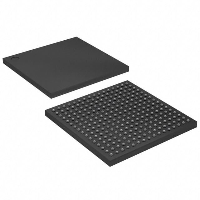
The via-in-PAD is an important part of the multilayer PCB. It not only bears the performance of the main functions of the PCB, but also uses the via-in-PAD to save space.The following is about VIA in PAD PCB related, I hope to help you better understand VIA in PAD PCB.

Buried vias: Buried vias only connect the traces between the inner layers, so they are not visible from the PCB surface. Such as 8layer board, the holes of 2-7 layers are buried holes.The following is about Mechanical Blind Buried Hole PCB related, I hope to help you better understand Mechanical Blind Buried Hole PCB.

20layer 5G PCB--The increase in the density of integrated circuit packaging has led to a high concentration of interconnect lines, which makes the use of multiple substrates a necessity. In the layout of the printed circuit, unforeseen design problems have appeared, such as noise, stray capacitance, and crosstalk. The following is about 20 layer Pentium Motherboard related, I hope to help you better understand 20-layer PCB.

Any integrated circuit is a monolithic module designed to complete certain electrical characteristics. IC testing is the test of integrated circuits, which uses various methods to detect those that do not meet the requirements due to physical defects in the manufacturing process. sample. If there are non-defective products, the testing of integrated circuits is not necessary.The following is about IC Test PCB related, I hope to help you better understand IC Test PCB.

IC testing is generally divided into physical Visual Inspecting Test, IC Functional Test, De-Capsulation, Solderbili, ty Test, Electrical Test, X-Ray, Rohs and FA.The following is about Large size EM-890K PCB related, I hope to help you better understand Large size EM-890K PCB.

Large size coil PCB--The coil usually refers to a wire winding in a loop. The most common coil applications are: motors, inductors, transformers, and loop antennas. The coil in the circuit refers to the inductor.The following is about 10 Layer Oversized Coil Board related, I hope to help you better understand 10-Layers Coil PCB.