HONTEC is one of leading Multilayer PCB manufacture, who specializes in high-mix,low volume and quickturn prototype PCB for high-tech industries in 28 countries.
Our Multilayer PCB has passed UL, SGS and ISO9001 certification, we are in application of ISO14001 and TS16949 as well.
Located in Shenzhen of GuangDong, HONTEC partners up with UPS, DHL and world-class forwarders to provide efficient shipping services. Welcome to buy Multilayer PCB from us. Every request from customers is being replied within 24 hours.

EM-890K2 PCB--The manufacturing method of multilayer board is generally made by the inner layer pattern first, and then the single or double-sided substrate is made by printing and etching method, which is included in the specified interlayer, and then heated, pressurized and bonded. As for the subsequent drilling, it is the same as the plating through-hole method of double-sided board.

EM-888K PCB--The manufacturing method of multilayer board is generally made by the inner layer pattern first, and then the single or double-sided substrate is made by printing and etching method, which is included in the designated interlayer, and then heated, pressurized and bonded. As for the subsequent drilling, it is the same as the plating through-hole method of double-sided plate. It was invented in 1961.

ultra small size coil PCB--Compared with the module board, the coil board is more portable, small in size and light in weight. It has a coil that can be opened for easy access and a wide frequency range. The circuit pattern is mainly winding, and the circuit board with etched circuit instead of traditional copper wire turns is mainly used in inductive components. It has a series of advantages such as high measurement, high accuracy, good linearity, and simple structure.The following is about 17 layers ultra small size coil board, I hope to help you better understand 17 layers ultra small size coil board.

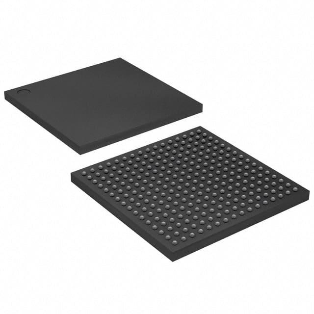
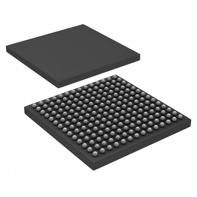
BGA is a small package on a pcb circuit board, and BGA is a packaging method in which an integrated circuit uses an organic carrier board.The following is about 8 layers EM-890 PCB, I hope to help you better understand 8 layers EM-890 PCB.

In the touch era, EM-370 PCB have been applied to various industrial equipment, such as industrial automation, gas station terminals, aircraft display screens, automotive GPS, medical equipment, bank POS and ATM machines, industrial measuring instruments, and high-speed rails, etc. Wait, a new industrial revolution is unfolding.The following is about4 layer EM-370 PCB, I hope to help you better understand 4 layer EM-370 PCB.

At high speeds, Impedance control PCB traces are used as transmission lines, and electrical energy can be reflected back and forth, similar to the situation where ripples in lake water encounter obstacles. Controlled impedance traces are designed to reduce electronic reflections and ensure correct conversion between PCB traces and internal connections.