Internet of Things Module HDI PCB Manufacturers

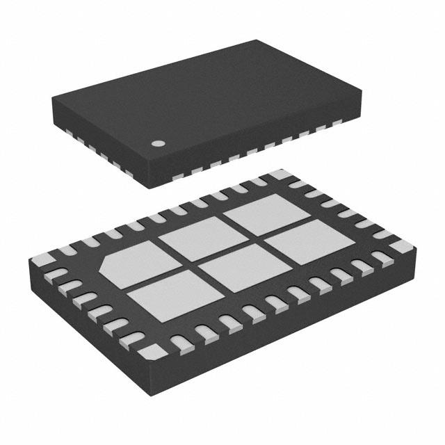
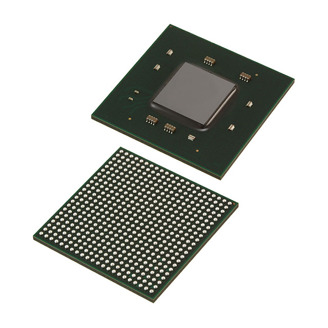
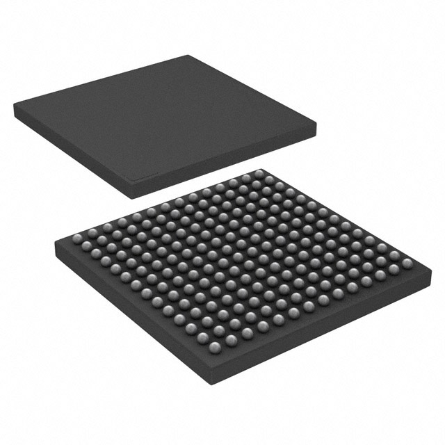
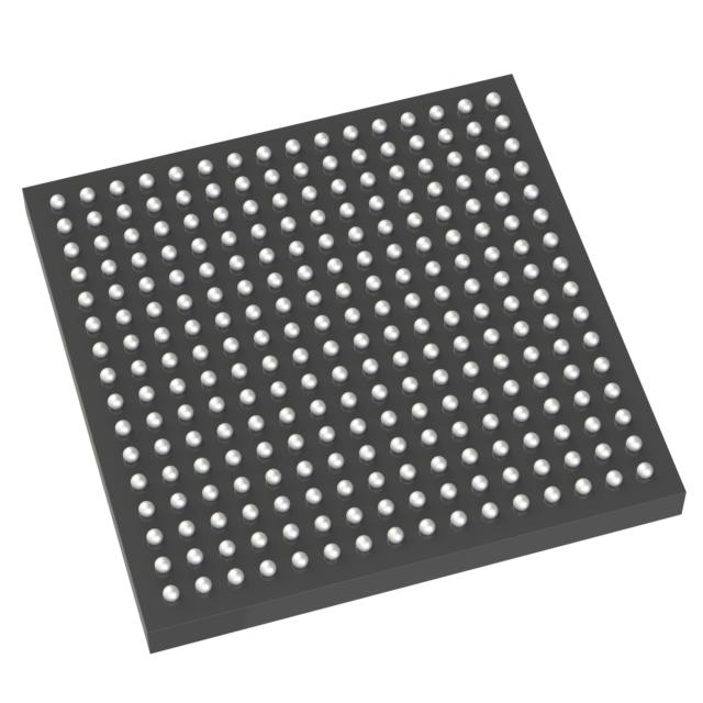
Our firm insists all along the quality policy of "product high quality is base of organization survival; consumer fulfillment could be the staring point and ending of an company; persistent improvement is eternal pursuit of staff" along with the consistent purpose of "reputation 1st, purchaser first" for Internet of Things Module HDI PCB,Bluetooth module HDI PCB,WIFI module HDI PCB,Bluetooth Module PCB, With us your money in risk-free your company in safe and sound . Hope we are able to be your trustworthy supplier in China . Seeking forward for your cooperation .
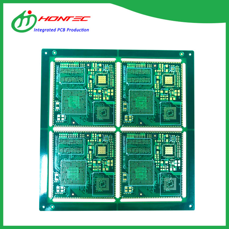
Internet of Things Module HDI PCB, With its rich manufacturing experience, high-quality products, and perfect after-sale service, the company has gained good reputation and has become one of the famous enterprise specialized in manufacturing series.We sincerely hope to establish business relation with you and pursue mutual benefit.

Hot Products

  • XC6SLX75-2FGG484C

    XC6SLX75-2FGG484C

    ​XC6SLX75-2FGG484C The platform's components support up to 150K logic density, 4.8Mb memory, integrated storage controllers, and easy-to-use high-performance system IPs (such as DSP modules), while adopting innovative open standard based configurations.
  • XCKU085-2FLVA1517I

    XCKU085-2FLVA1517I

    ​XCKU085-2FLVA1517I has a power option to achieve the best balance between required system performance and low-power envelope. XCKU085-2FLVA1517I is an ideal choice for packet processing and DSP intensive features, suitable for various applications from wireless MIMO technology to Nx100G networks and data centers.
  • XC7VX690T-2FFG1927C

    XC7VX690T-2FFG1927C

    XC7VX690T-2FFG1927C is a low-cost field-programmable gate array (FPGA) developed by Intel Corporation, a leading semiconductor technology company. This device features 120,000 logic elements and 414 user input/output pins, making it suitable for a wide range of low-power and low-cost applications. It operates on a single power supply voltage ranging from 1.14V to 1.26V and supports various I/O standards such as LVCMOS, LVDS, and PCIe. The device has a maximum operating frequency of up to 415 MHz. The device comes in a small fine pitch ball grid array (FGBA) package with 484 pins, providing high pin-count connectivity for a variety of applications.
  • B50292B0KQLEG

    B50292B0KQLEG

    B50292B0KQLEG is suitable for use in a variety of applications, including industrial control, telecommunications, and automotive systems. The device is known for its easy-to-use interface, high efficiency, and thermal performance, making it an ideal choice for a wide range of power management applications.
  • BCM82072BKFSBG

    BCM82072BKFSBG

    BCM82072BKFSBG is suitable for use in a variety of applications, including industrial control, telecommunications, and automotive systems. The device is known for its easy-to-use interface, high efficiency, and thermal performance, making it an ideal choice for a wide range of power management applications.
  • RO3003 PCB

    RO3003 PCB

    The delay per unit inch on the PCB is 0.167ns. However, if there are more vias, more device pins, and more constraints set on the network cable, the delay will increase. Generally, the signal rise time of high-speed logic devices is about 0.2ns. If there are GaAs chips on the board, the maximum wiring length is 7.62mm. The following is about RO3003 PCB related, I hope to help you better understand RO3003 PCB.

Send Inquiry