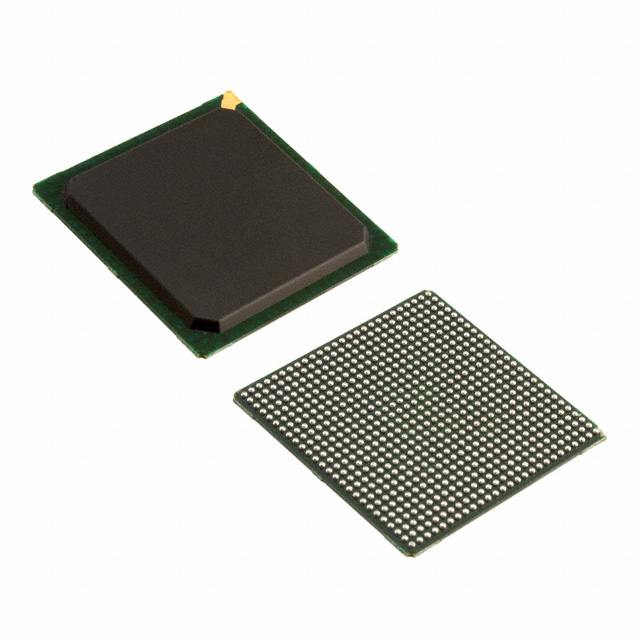
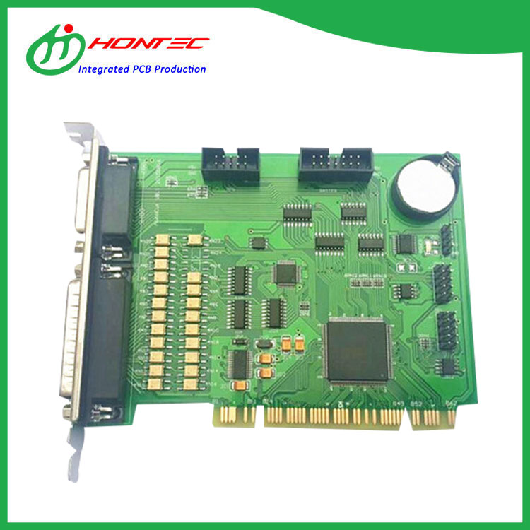
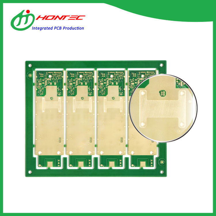
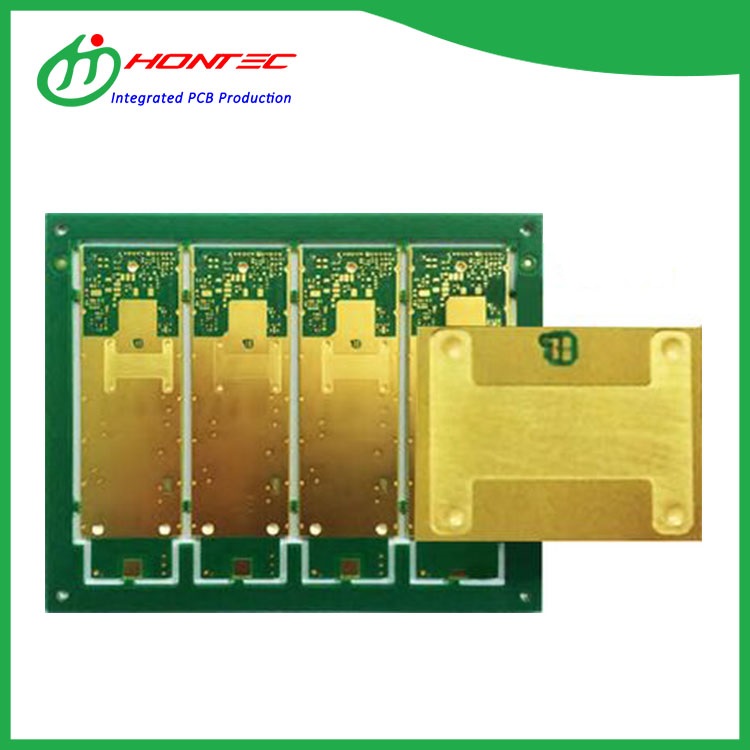
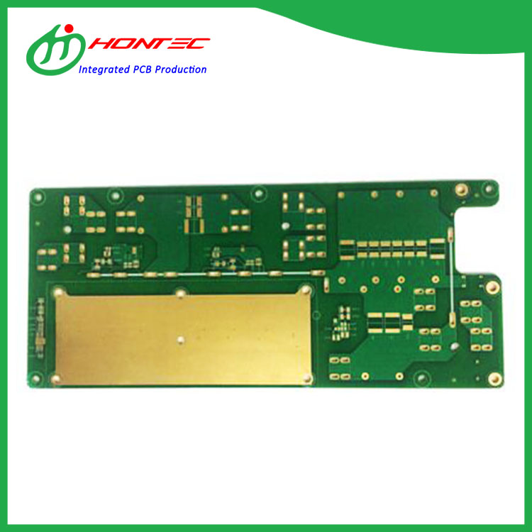
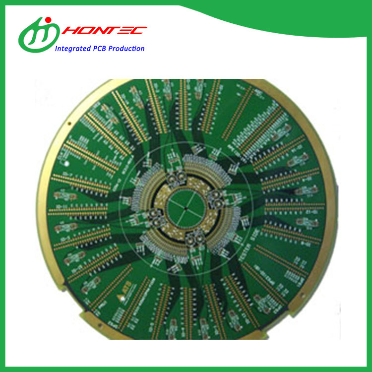
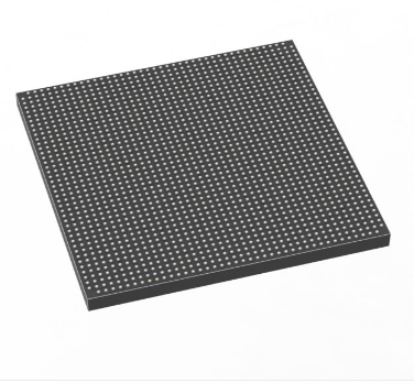
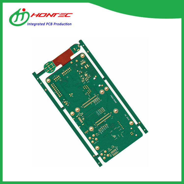
Well-run gear, qualified revenue workforce, and superior after-sales companies; We've been also a unified huge loved ones, anyone persist with the organization benefit "unification, determination, tolerance" for Inlaid copper Coin PCB,built-in Copper Coin PCB,Buried copper Coin PCB, We fully welcome shoppers from all around the world to ascertain stable and mutually effective enterprise interactions, to have a dazzling long run jointly.
Inlaid copper Coin PCB, We hope to have long-term cooperation relationships with our clients. If you are interested in any of our items, be sure to do not hesitate to send enquiry to us/company name. We ensure that you can be totally satisfied with our best solutions!