26 layers of 2step HDI PCB Manufacturers

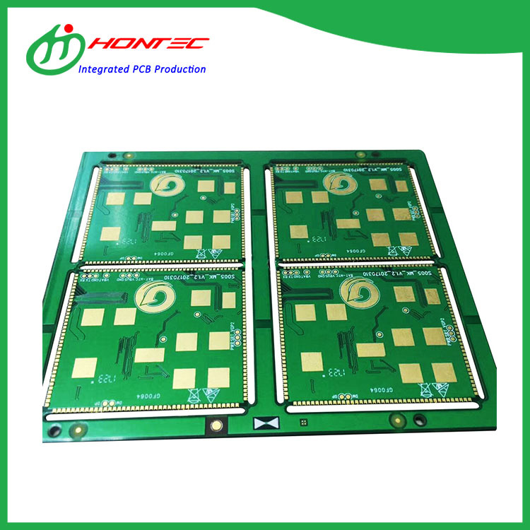
Using a complete scientific high quality management program, superior high quality and superior faith, we acquire great reputation and occupied this industry for 26 layers of 2step HDI PCB,24 layers ELIC HDI PCB,22 layers of 3step HDI PCB, 1st business enterprise, we find out each other. Even further business enterprise, the trust is getting there. Our enterprise always at your services at any time.
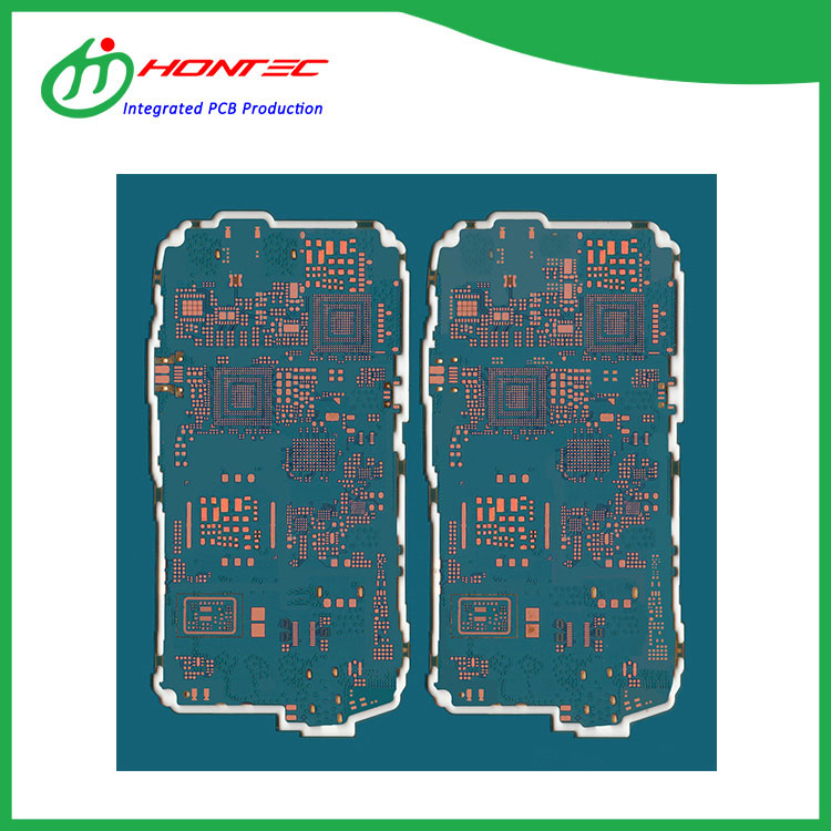
26 layers of 2step HDI PCB, Although continuous opportunity, now we have now developed serious a friendly relationship with many oversea merchants, such as ones through Virginia. We securely assume that the merchandise regarding t shirt printer machine is often good through a great number of having its good quality and also cost.

Hot Products

  • XCF01SV0G20C

    XCF01SV0G20C

    XCF01SV0G20C is suitable for use in a variety of applications, including industrial control, telecommunications, and automotive systems. The device is known for its easy-to-use interface, high efficiency, and thermal performance, making it an ideal choice for a wide range of power management applications.
  • N9000-13RF PCB

    N9000-13RF PCB

    N9000-13rf PCB is a RF substrate developed by nelco company in Singapore. It is FR4 and easy to process. Its application field is usually communication industry
  • XC7A35T-2CSG325I

    XC7A35T-2CSG325I

    XC7A35T-2CSG325I is suitable for use in a variety of applications, including industrial control, telecommunications, and automotive systems. The device is known for its easy-to-use interface, high efficiency, and thermal performance, making it an ideal choice for a wide range of power management applications.
  • XCVU13P-2FHGA2104I

    XCVU13P-2FHGA2104I

    XCVU13P-2FHGA2104I is a scalable and reconfigurable acceleration platform suitable for optimizing complex workloads. It has a large amount of raw computing power and I/O flexibility, suitable for computationally intensive workloads in data center applications
  • Cross Blind Buried Hole PCB

    Cross Blind Buried Hole PCB

    PCB, also called printed circuit board, printed circuit board. Multi-layer printed board refers to a printed board with more than two layers. It is composed of connecting wires on several layers of insulating substrates and pads for assembling and soldering electronic components. The role of insulation.The following is about Cross Blind Buried Hole PCB related, I hope to help you better understand Cross Blind Buried Hole PCB.
  • MT41K512M16HA-107:A

    MT41K512M16HA-107:A

    MT41K512M16HA-107:A is suitable for use in a variety of applications, including industrial control, telecommunications, and automotive systems. The device is known for its easy-to-use interface, high efficiency, and thermal performance, making it an ideal choice for a wide range of power management applications.

Send Inquiry