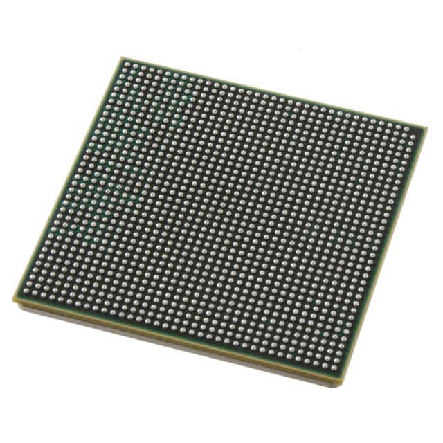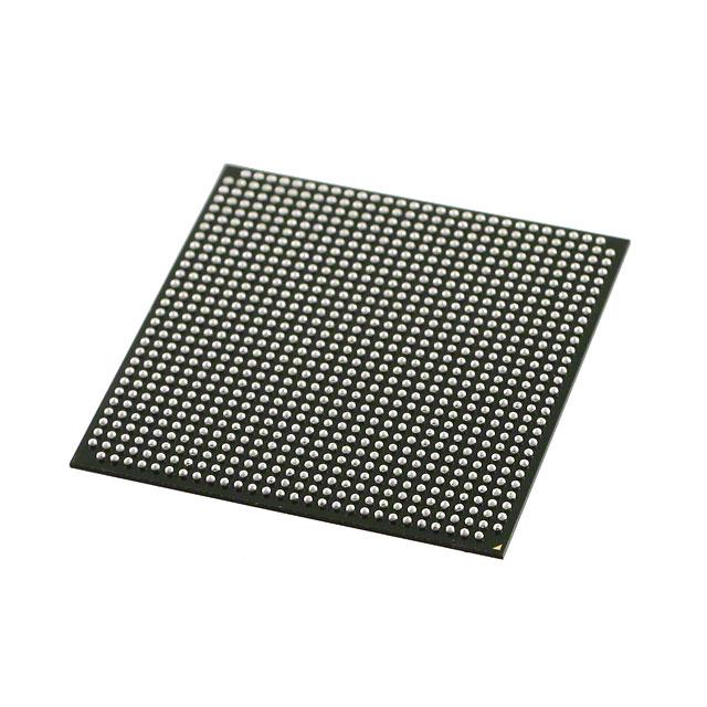

Electronic design is constantly improving the performance of the whole machine, but also trying to reduce its size. From mobile phones to smart weapons, "small" is the eternal pursuit. High density integration (HDI) technology can make terminal product design more miniaturized, while meeting higher standards of electronic performance and efficiency. Welcome to buy 6-Layer HDI PCB from us.

HDI PCB is the abbreviation of "high density interconnector", which is a kind of printed circuit board (PCB) production. It is a kind of circuit board with high line distribution density using micro blind buried hole technology.

High frequency step PCB With the small and diversified development of electronic products, restricted by the space and security, the traditional plane circuit board can not meet the requirements of many fields of electronic products, and more and more step PCB has been gradually developed.

copper paste filled hole PCB: Bai AE3030 copper pulp is a non-conductive DAO copper paste used for the high-density assembly of printed substrate DU plate and the laying of wires.Due to the characteristics of Zhuan "high Thermal conductivity", "bubble-free", "flat" and so on, the copper paste is most suitable for the design of high reliability Pad on Via, stack on Via and Thermal Via. The copper paste is widely used from aerospace satellite, server, cabling machine, LED backlight and so on.

EM-526 High-speed PCB, with the rapid development of electronic technology, more and more large-scale integrated circuits (LSI) are used. At the same time, the use of deep submicron technology in IC design makes the integration scale of the chip larger.

18 layers copper paste plug hole PCB realizes high-density assembly of printed circuit boards and non-conductive copper paste for via plug holes of wiring. It is widely used in aviation satellites, servers, wiring machines, LED backlights, etc.The following is about 18 layers copper paste plug hole, I hope to help you better understand 18 layers copper paste plug hole.