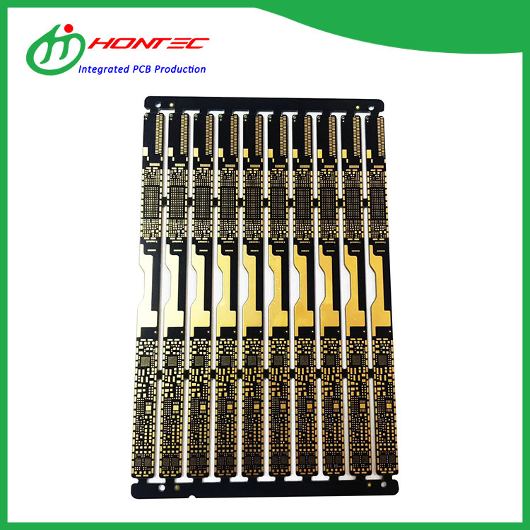
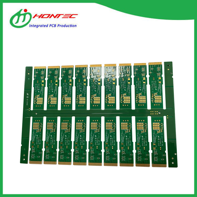
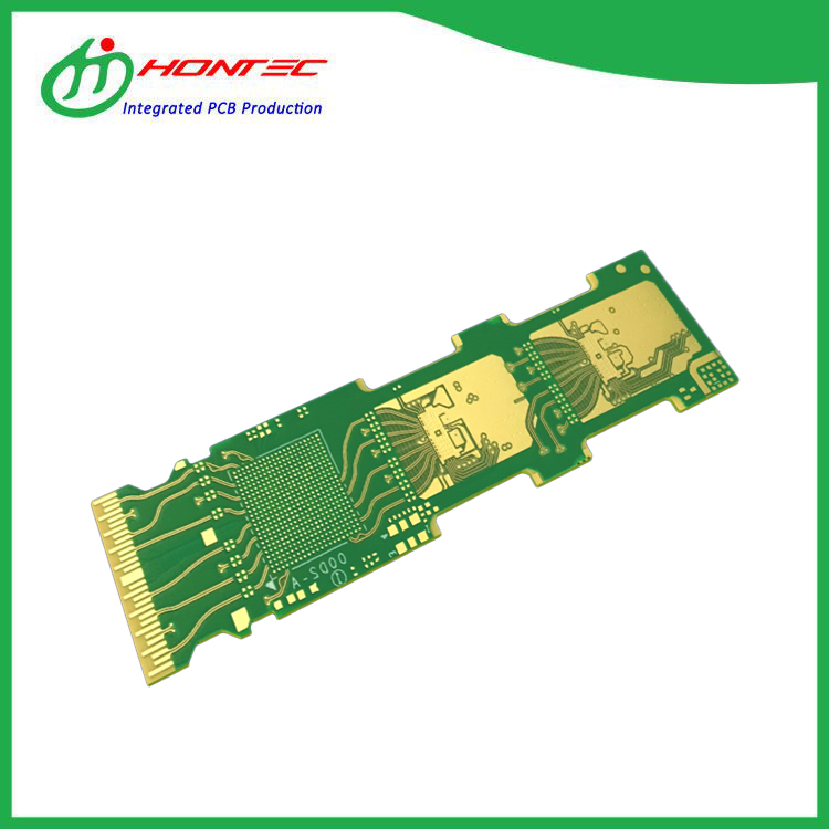
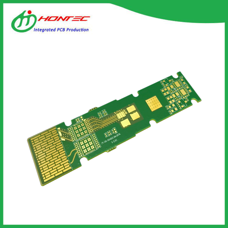
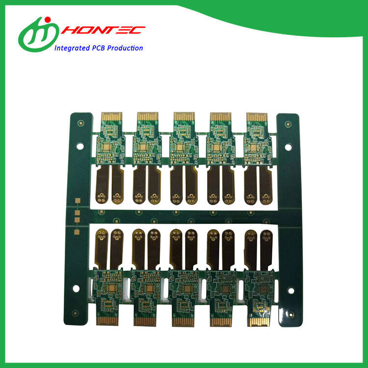
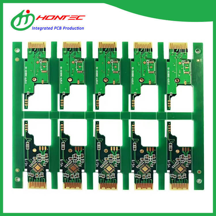
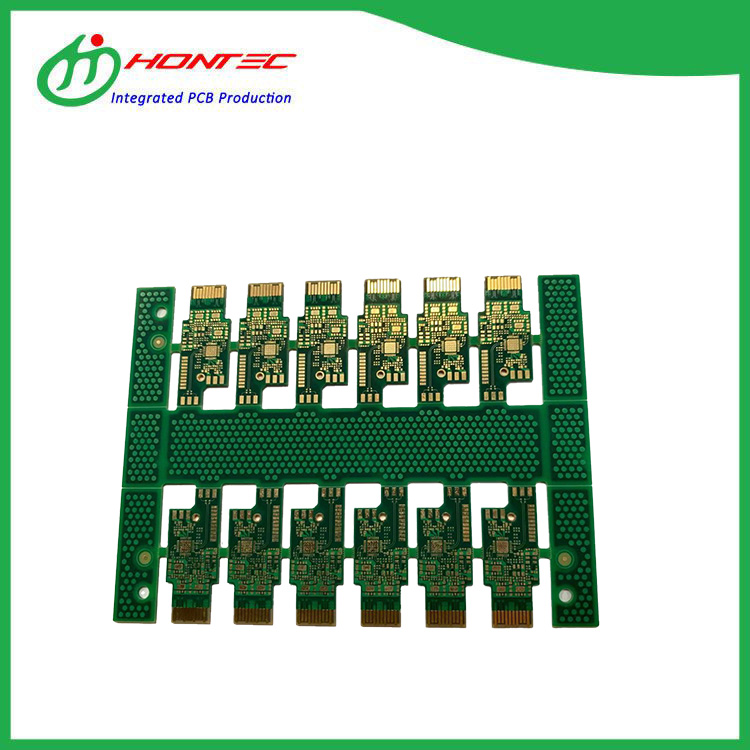
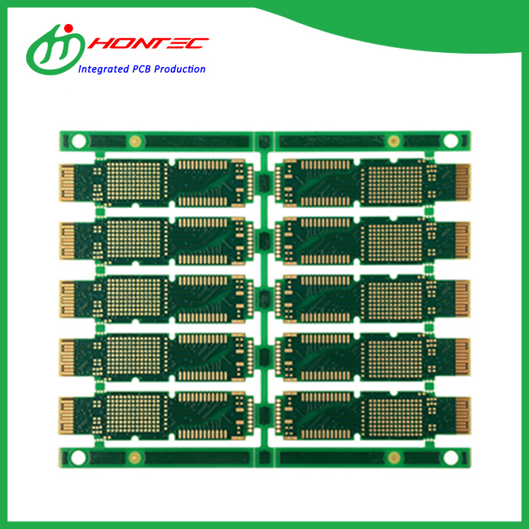
The 200G optical module PCB is composed of shell, PCBA (PCB blank board + driver chip) and optical devices (dual fiber: Tosa, Rosa; single fiber: Bosa). In short, the function of the optical module is photoelectric conversion. The transmitter converts the electrical signal into the optical signal, and then the receiver converts the optical signal into the electrical signal after transmission through the optical fiber.
100G optoelectronic PCB is a packaging substrate for a new generation of high computing, which integrates light with electricity, transmits signals with light and operates with electricity. It adds a layer of light guide to the traditional printed circuit board, which is very mature at present.
The pace of the 400g network is getting closer and closer. The domestic Internet giants Alibaba and Tencent plan to start upgrading the 400g network in 2019. The 400G optical module PCB, as the hardware of the 400G network upgrade, has attracted the attention of all parties.
The main function of 40G optical module PCB is to realize photoelectric and electro-optic transformation, including optical power control, modulation and transmission, signal detection, IV conversion and limiting amplification judgment regeneration. In addition, there are anti-counterfeiting information query, TX disable and other functions. The common functions are: SFF, SFF, GBP +, GBIC, XFP, 1x9, etc.
The function of the Optical module PCB is to convert the electrical signal into optical signal at the sending end, and then convert the optical signal into the electrical signal at the receiving end after transmitting through the optical fiber.
2.5G optical module PCB--The function of the optical module is photoelectric conversion. The transmitting end converts the electrical signal into an optical signal. After transmission through the optical fiber, the receiving end converts the optical signal into an electrical signal.The following is about 2.5G Optical Module PCB related, I hope to help you better understand 2.5G Optical Module PCB.