IMX334LQR-C is suitable for use in a variety of applications, including industrial control, telecommunications, and automotive systems. The device is known for its easy-to-use interface, high efficiency, and thermal performance, making it an ideal choice for a wide range of power management applications.

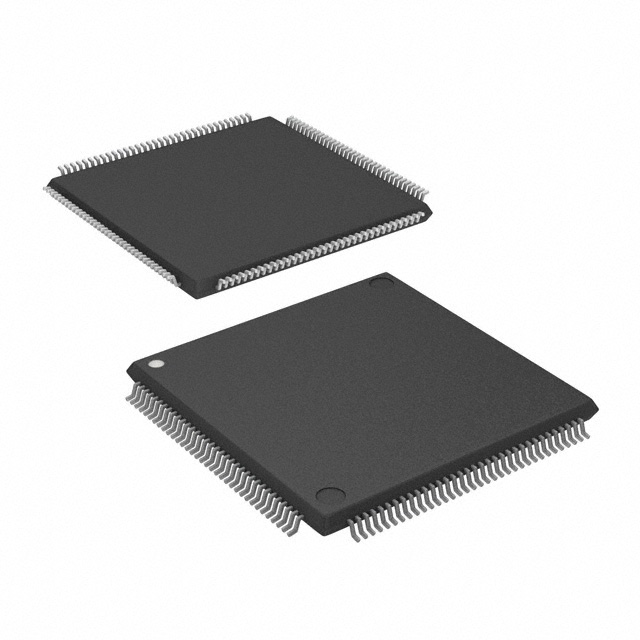
EPM240M100I5N is suitable for use in a variety of applications, including industrial control, telecommunications, and automotive systems. The device is known for its easy-to-use interface, high efficiency, and thermal performance, making it an ideal choice for a wide range of power management applications.

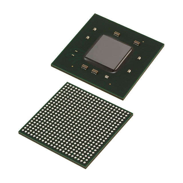
XCZU3EG-2SFVA625I is suitable for use in a variety of applications, including industrial control, telecommunications, and automotive systems. The device is known for its easy-to-use interface, high efficiency, and thermal performance, making it an ideal choice for a wide range of power management applications.

AD9652BBCZ-310 is suitable for use in a variety of applications, including industrial control, telecommunications, and automotive systems. The device is known for its easy-to-use interface, high efficiency, and thermal performance, making it an ideal choice for a wide range of power management applications.

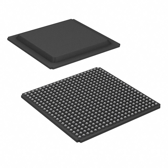
10AX027E3F27I2LG is suitable for use in a variety of applications, including industrial control, telecommunications, and automotive systems. The device is known for its easy-to-use interface, high efficiency, and thermal performance, making it an ideal choice for a wide range of power management applications.

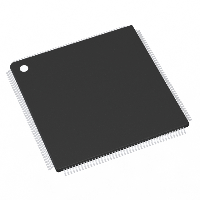
10AS027E3F27I2LG is suitable for use in a variety of applications, including industrial control, telecommunications, and automotive systems. The device is known for its easy-to-use interface, high efficiency, and thermal performance, making it an ideal choice for a wide range of power management applications.