In 1936, Austrian Paul Eisler first used printed circuit board in radio. In 1943, Americans mostly applied this technology to military radios. In 1948, the United States officially recognized that this invention can be used for commercial purposes. Since the mid-1950s, printed circuit boards have been widely used.
Before the emergence of PCB, the interconnection between electronic components was completed by direct connection of wires. Nowadays, wires only exist in the laboratory for experimental application; Printed circuit board has certainly occupied the position of absolute control in the electronic industry.
In order to increase the area of wiring, multilayer boards use more single and double-sided wiring boards. A printed circuit board with one double-sided as the inner layer, two single-sided as the outer layer, or two double-sided as the inner layer and two single-sided as the outer layer, which is alternately connected together through the positioning system and insulating bonding materials, and the conductive graphics are interconnected according to the design requirements, becomes a four layer and six layer printed circuit board, also known as multi-layer printed circuit board.
Copper clad laminate is the substrate material for making printed circuit board. It is used to support various components and can realize electrical connection or electrical insulation between them.
From the beginning of the 20th century to the end of the 1940s, a large number of resins, reinforcing materials and insulating substrates for substrate materials emerged, and the technology has been preliminarily explored. All these have created necessary conditions for the emergence and development of Zui typical substrate material for printed circuit board - copper clad laminate. On the other hand, PCB manufacturing technology with metal foil etching (subtraction) as the mainstream has been Zui initially established and developed. It plays a decisive role in determining the structural composition and characteristic conditions of copper clad laminate.
In the printed circuit board, lamination is also called "lamination", which overlaps the inner single sheet, semi cured sheet and copper foil and is pressed into multilayer board at high temperature. For example, a four ply board needs to be pressed by one inner single sheet, two copper foils and two groups of semi cured sheets.
The drilling process of Multilayer PCB is generally not completed at one time, which is divided into one drill and two drills.
One drill requires copper sinking process, that is, copper is plated in the hole, so that the upper and lower layers can be connected, such as through hole, original hole, etc.
The second drilled hole is the hole that does not need copper sinking, such as screw hole, positioning hole, heat dissipation groove, etc. the pocket in these holes does not need copper.
Film is an exposed negative. The PCB surface will be coated with a layer of photosensitive liquid, dried after 80 degrees of temperature test, then pasted on the PCB board with film, exposed by ultraviolet exposure machine and torn off the film. The circuit diagram is presented on the PCB.
Green oil refers to the ink coated on copper foil on PCB. This layer of ink can cover unexpected conductors except bonding pads, avoid welding short circuit and prolong the service life of PCB in the process of use; It is generally called resistance welding or anti welding; The colors are green, black, red, blue, yellow, white, matte, etc. Most PCBs use green solder resist ink, which is usually called green oil.
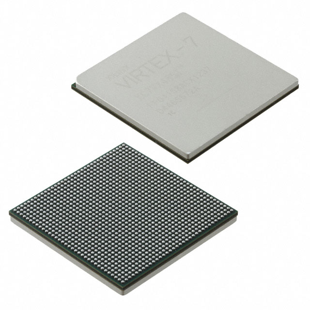
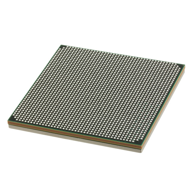
The plane of the computer motherboard is a PCB (printed circuit board), which generally adopts four layer board or six layer board. Relatively speaking, in order to save costs, low-grade mainboards are mostly four layers: main signal layer, grounding layer, power layer and secondary signal layer, while six layers add auxiliary power layer and medium signal layer. Therefore, the mainboard of six layers PCB has stronger anti electromagnetic interference ability and more stable mainboard