PCB manufacturers show you the evolution of PCB production process. In the 1950s and early 1960s, laminates mixed with different types of resins and various materials were introduced, but PCB is still single-sided. The circuit is on one side of the circuit board and the component is on the other side. Compared with the huge wiring and cable, PCB has become the first choice for new products to enter the market. But the biggest impact on the evolution of printed circuit boards comes from the government agencies responsible for new weapons and communication equipment. Wire end components are used in some applications. Initially, the lead of the component is fixed to the circuit board by using a small nickel plate welded to the lead.
Finally, the process of copper plating on the borehole wall was developed. This allows the circuits on both sides of the board to be electrically connected. Copper has replaced brass as the preferred metal because of its current carrying capacity, relatively low cost and easy manufacture. In 1956, the U.S. Patent Office issued a patent for the "process of assembling circuits" sought by a group of scientists represented by the U.S. Army. The patented process involves the use of base materials such as melamine, in which a layer of copper foil has been firmly laminated. Draw the wiring pattern and shoot it on the zinc plate. The plate is used to make the printing plate of offset press. The acid resistant ink is printed on the copper foil side of the plate, which is etched to remove the exposed copper, leaving a "printing line". Other methods are also proposed, such as using templates, screening, manual printing and rubber embossing to deposit ink patterns. Then use the die to punch the hole into a pattern to match the position of the component lead or terminal. Insert the lead through a non electroplated hole in the laminate, and then immerse or float the card on the molten solder bath. The solder will coat the trace and connect the lead of the component to the trace. Manual printing and rubber embossing are also proposed to deposit ink patterns. Then use the die to punch the hole into a pattern to match the position of the component lead or terminal. Insert the lead wire through the non plating bath or into the floating card. The solder will coat the trace and connect the lead of the component to the trace. Manual printing and rubber embossing are also proposed to deposit ink patterns. Then use the die to punch the hole into a pattern to match the position of the component lead or terminal. Insert the lead through a non electroplated hole in the laminate, and then immerse or float the card on the molten solder bath. The solder will coat the trace and connect the lead of the component to the trace.
They also use tinned eyelets, rivets and washers to connect various types of components to the circuit board. Their patent even has a drawing showing two single panels stacked together and a bracket to separate them. There are components at the top of each board. The lead of one component extends through the hole on the top plate and the bottom plate, connects them together, and roughly tries to make the first multilayer board.
Since then, the situation has changed greatly. With the emergence of electroplating process that allows hole wall plating, the first double-sided plate appeared. Our surface mount pad technology related to the 1980s was actually explored in the 1960s. Solder masks have been used since 1950 to help reduce traces and corrosion of components. Epoxy compounds are spread on the surface of the assembly board, similar to what we now know as conformal coatings. Finally, before assembling the circuit board, the ink is screen printed on the panel. The area to be welded is blocked on the screen. It helps keep the circuit board clean and reduces corrosion and oxidation, but the tin / lead coating used to apply traces will melt during welding, resulting in mask peeling. Due to the wide spacing of traces, it is regarded as a cosmetic problem rather than a functional problem. By the 1970s, the circuit and spacing became smaller and smaller, and the tin / lead coating used to coat the traces on the circuit board began to fuse the traces together during the welding process.
The hot air welding method began in the late 1970s and allowed the stripping of tin / lead after etching to eliminate problems. A welding mask can then be applied to the bare copper circuit, leaving only plated holes and pads to avoid coating solder. As the holes continue to get smaller, the trace work becomes more intensive, and the bleeding and registration problems of the welding mask bring about the dry film mask. They are mainly used in the United States, and the first imageable masks are being developed in Europe and Japan. In Europe, solvent based "probimer" inks are applied by curtain coating the entire panel. Japan focuses on screening methods using various aqueous developing LPI. All three of these mask types use standard UV exposure units and photo tools to define patterns on the panel. By the mid-1990s'
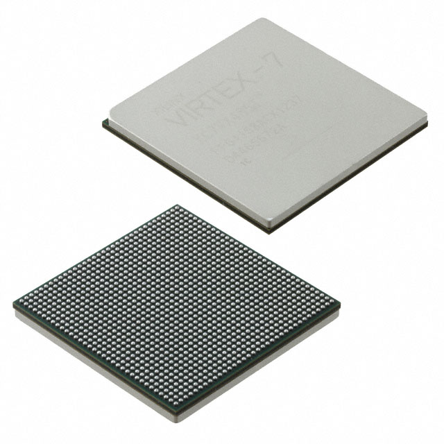
The increase in complexity and density leading to the development of welding masks also forces the development of copper trace layers stacked between dielectric material layers. 1961 marked the first use of multilayer circuit boards in the United States. The development of transistors and the miniaturization of other components have attracted more and more manufacturers to use printed circuit boards for more and more consumer products. Aerospace equipment, flight instruments, computer and telecommunications products, as well as defense systems and weapons, have begun to take advantage of the space savings provided by multilayer circuit boards. The size and weight of the surface mount device being designed are equivalent to comparable through-hole components. With the invention of integrated circuit, the circuit board is shrinking in almost all aspects. Rigid board and cable applications have given way to flexible circuit boards or rigid flexible combination circuit boards. These and other advances will make printed circuit board manufacturing a dynamic field for many years