1. Poor wetting
Poor wetting means that the solder and the soldering area of the substrate during the soldering process will not generate inter-metal repercussions after being moistened, and will result in missed soldering or less soldering defects. Most of the reasons are that the surface of the solder area is contaminated, or is stained with solder resist, or a metal compound layer is formed on the surface of the bonded object. For example, there are sulfides on the surface of silver, and oxides on the surface of tin will cause wetting. bad. In addition, when the residual aluminum, zinc, cadmium, etc. in the soldering process exceeds 0.005%, the moisture absorption effect of the flux reduces the activity level, and poor wetting may also occur. In wave soldering, if there is gas on the surface of the substrate, this problem is also prone to occur. Therefore, in addition to performing appropriate soldering processes, anti-fouling measures must be taken for the appearance of the substrate and the appearance of the components, selecting suitable solders, and setting reasonable soldering temperature and time.
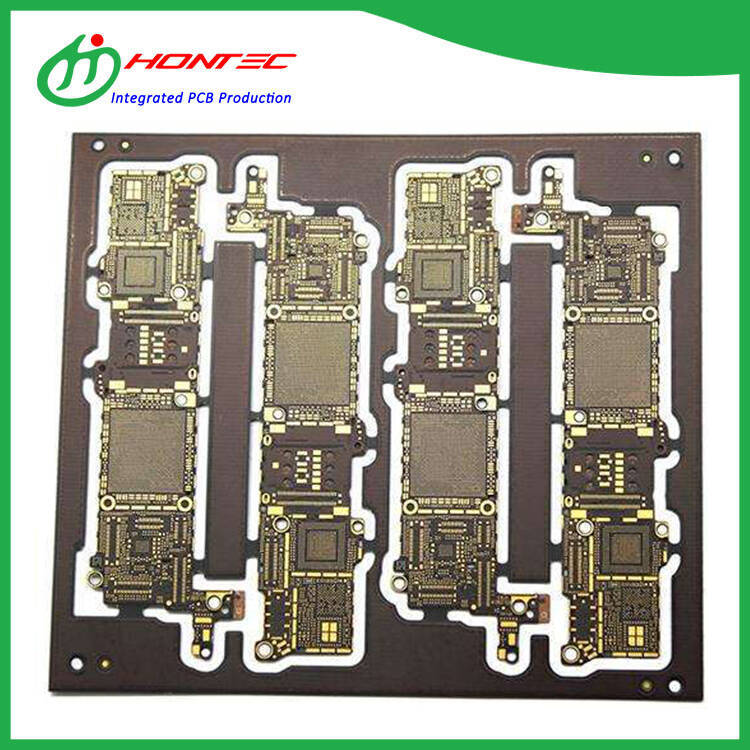
PCB surface mount soldering
2. Bridge Union
The causes of bridging are mostly caused by excessive solder or severe edge collapse after solder printing, or the size of the substrate solder area is out of tolerance, SMD placement offset, etc., when SOP and QFP circuits tend to be miniaturized, bridging will be formed Electrical short circuit affects the use of products.
As a correction method:
(1)To avoid bad edge collapse during solder paste printing.
(2)The size of the soldering area of the substrate should be set to meet the design requirements.
(3)The mounting position of SMD must be within the scope of the rules.
(4)The wiring gap of the substrate and the coating accuracy of the solder resist must meet the requirements of the rules.
(5)Develop appropriate welding technical parameters to avoid mechanical vibration of the welding machine conveyor belt.
3. Solder ball
The occurrence of solder balls is usually caused by the rapid heating during the soldering process and the scattering of the solder. Others are misaligned with the printing of the solder and collapsed. Pollution, etc. are also related.
Measures to avoid:
(1)To avoid over-rapid and bad welding heating, carry out welding according to the set heating technology.
(2)Implement the corresponding preheating technology according to the welding type.
(3)Defects such as solder bumps and misalignments should be deleted.
(4)The application of solder paste should meet the demand without bad moisture absorption.
4.crack
When the soldered
PCB just leaves the soldering zone, due to the difference in thermal expansion between the solder and the joined parts, under the effect of rapid cooling or rapid heating, due to the effect of condensation stress or shortening stress, the SMD will fundamentally crack. In the process of punching and transportation, it is also necessary to reduce the impact stress on SMD. Bending stress.
When designing exterior-mounted products, you should consider reducing the distance of thermal expansion, and accurately set heating and other conditions and cooling conditions. Use solder with excellent ductility.
5. Suspension bridge
Poor suspension bridge refers to the fact that one end of the component is separated from the soldering area and stands upright or upright. The cause of the occurrence is that the heating speed is too fast, the heating direction is not balanced, the selection of solder paste is questioned, the preheating before soldering, and the size of the soldering area, The shape of SMD itself is related to wettability.
Measures to avoid:
1. The storage of SMD must meet the demand.
2. The printing thickness scale of solder should be set accurately.
3. Adopt a reasonable preheating method to achieve uniform heating during welding.
4. The scale of the length of the substrate welding area should be properly formulated.
5. Reduce the external tension on the end of the SMD when the solder melts.