The following five aspects are introduced to you:
1. Brief introduction of circuit board
2. Introduction of circuit board base materil
3. Basic stack structure of circuit board
4. Circuit board production process
 Brief introduction of circuit board
1. FlexPrintCircuit ,referred to as"FPC"
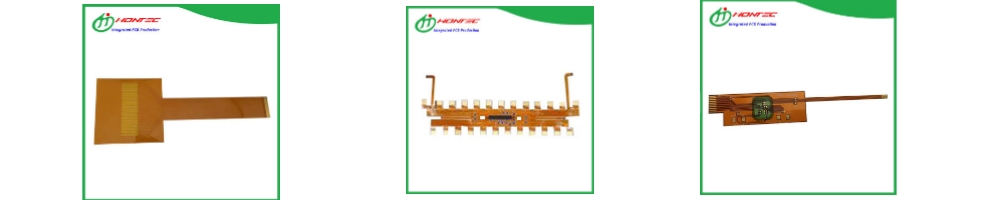
FPC is a single-layer, double-layer or multi-layer printed circuit board made of Flexible base material .FPC has light, thin, short, small, highThe characteristics of density, high stability and flexible structure, in addition to static bending, can also be used for dynamic bending, curling and folding.
2. Printed Circuie Board, referred to as "PCB"
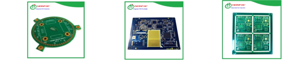
PCB printed circuit board made of rigid base material that is not easily deformed, and is flat when used. It has the advantages of high strength, not easy to warp, and firm installation of chip components.
3. Rigid Flex PCB
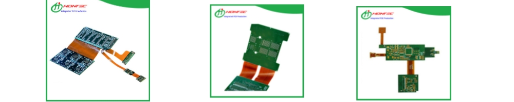
Rigid Flex PCB is a Printed Circuit Boards composed of rigid and flexible substrates laminated selectively together with a compact structure and metalized holes to form electrical connections. Rigid Flex PCB has the characteristics of high density, thin wire, small aperture, small size, light weight, high reliability, and its performance is still very stable under vibration, impact and humid environment. Flexible installation, three-dimensional installation and effective use of installation space are widely used in portable digital products such as mobile phones, digital cameras and digital video cameras. Rigid-flexible pcb will be used more in the field of packaging reduction, especially in the consumer field.
 Introduction of circuit board base materil
1. Conductive medium: copper (CU).
Copper foil: rolled copper (RA), electrolytic copper (ED), high ductility electrolytic copper (HTE)
Copper thickness: 1/4OZ, 1/3OZ, 1/2OZ, 1OZ, 2OZ, this is the more common thickness
Copper foil thickness unit: 1OZ = 1.4 mil
2. Insulation layer: Polyimide, Polyester, and PEN.
The more commonly used is polyimide (referred to as "PI")
PI thickness: 1/2mil, 1mil, 2mil,
The more common thickness is 1 mil = 0.0254mm = 25.4um = 1/1000 inch
3. Adhesive: epoxy resin system, acrylic system.
The more commonly used is the epoxy resin system, and the thickness varies according to different manufacturers.
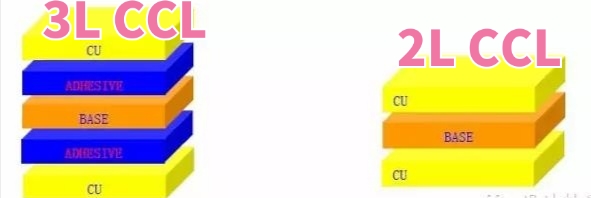
4. Copper clad laminates ("CCL" for short):
Single-sided copper clad laminate: 3L CCL (with glue), 2L CCL (without glue), the following is an illustration.
Double-sided copper clad laminate: 3L CCL (with glue), 2L CCL (without glue), the following is an illustration.
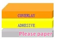
5. Coverlay (CVL)
It is composed of an insulating layer and an adhesive, and covers the wire to protect and insulate. The specific stack structure is as follows
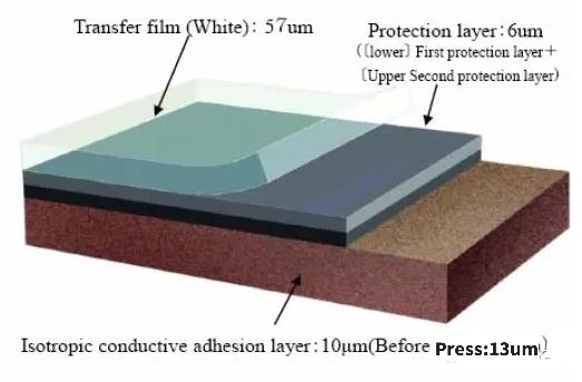
6. Conductive silver foil: electromagnetic wave protective film
Type: SF-PC6000 (black, 16um)
Advantages: ultra-thin, good sliding performance and deflection performance, suitable for high temperature reflow soldering, good dimensional stability.
Commonly used is SF-PC6000, the laminated structure is as follows:
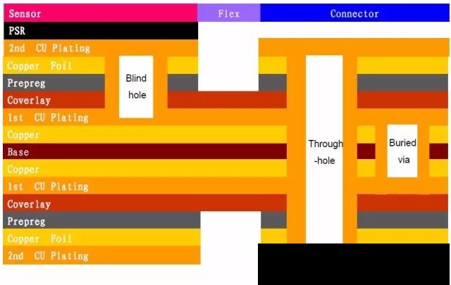
 Basic stack structure of circuit board
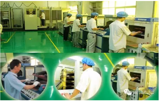
 Circuit board production process
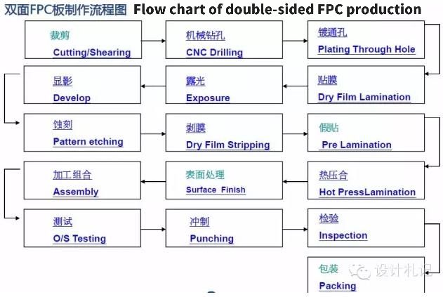
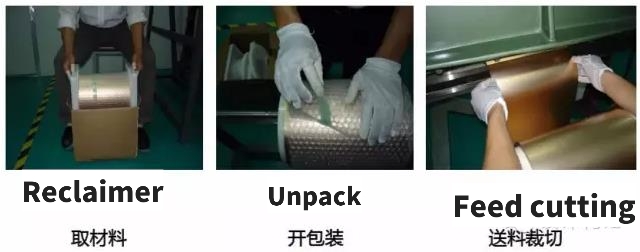
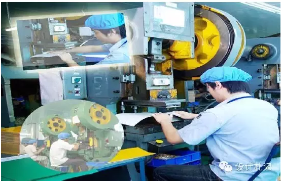
1.Cutting/Shearing
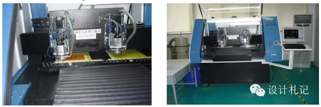
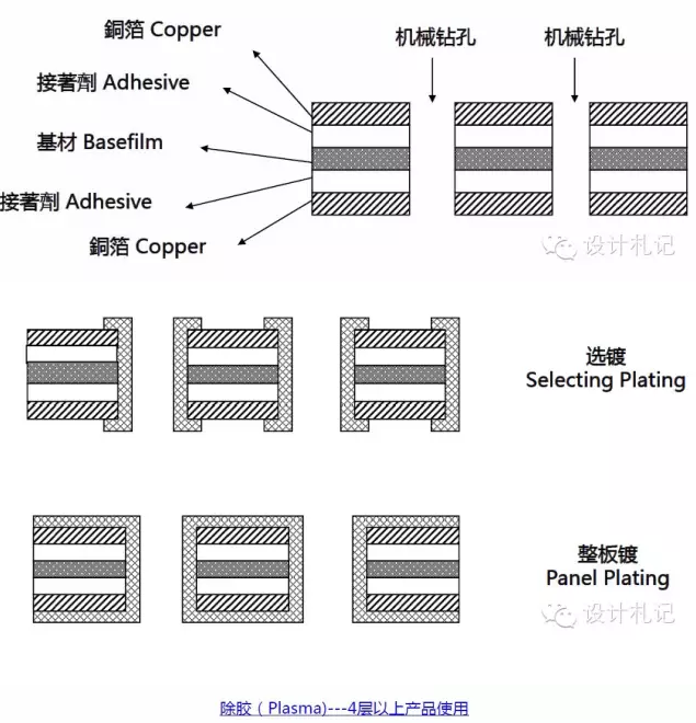
2.CNCDrilling
3.PlatingThroughHole
4.DES process
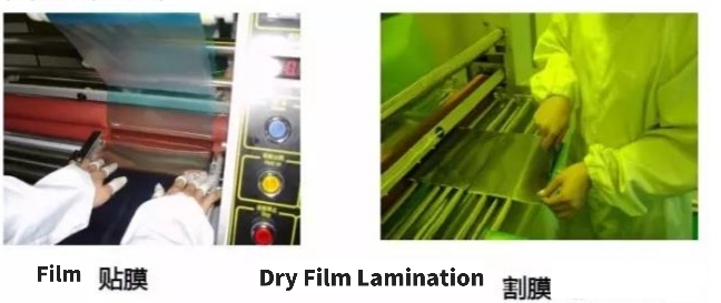
( 1)Film
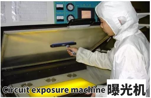
( 2)Exposure
Operating environment: Huang Guang
Purpose of the operation: Through UV light irradiation and film blocking, the film transparent area and the dry film will have an optical reaction. The film is brown, the UV light cannot penetrate, and the film cannot have an optical polymerization reaction with its corresponding dry film
( 3)Developing
Working solution: Na2CO3 (K2CO3) weak alkaline solution
Purpose of the operation: Use a weak alkaline solution to clean the dry film part that has not undergone polymerization
( 4 ) Etching
Working solution: acid oxygen water: HCl+H2O2
Purpose of the operation: Use the chemical solution to etch away the copper exposed after development to form a pattern transfer.
( 5 ) Stripping
Working solution: NaOH strong alkaline solution
5. AOI
Main equipment: AOI, VRS system
The formed copper foil must be scanned by the AOI system to detect the missing line. The standard line image information is stored in the AOI host in the form of data, and the line information on the copper foil is scanned into the host through the CCD optical pick-up head and compared with the stored standard data. When there is an abnormality, the location of the abnormal point will be transmitted to the VRS host by the number record ... The VRS will magnify the copper foil 300 times and display it in order according to the defect position recorded in advance. The operator will judge whether it is a true defect. For the true defect, a water-based pen will be used to mark the defect position. In order to facilitate the follow-up operators to classify and repair the defects. Operators use 150 times magnifying glass to judge
Types of shortcomings, classified statistics form quality reports, and feedback to the previous process to facilitate timely implementation of improvement measures. Because the single panel has fewer shortcomings and lower cost, it is difficult to use AOI to interpret, so it is directly inspected by artificial naked eyes.
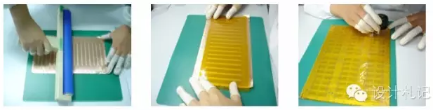
6. Fake stickers
Protective film function:
(1) Insulation and solder resistance;
(2) Protection circuit;
(3) Increase the flexibility of the flexible board.
7. Hot pressing
Operating conditions: high temperature and high pressure
8. Surface treatment
After hot pressing, surface treatment (gold-plated, tin-sprayed or OSP) is required on the exposed location of the copper foil. The method depends on customer requirements.
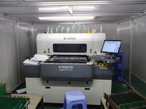
9. silk screen
Main equipment: screen printing machine. Oven. UV dryer. Screen printing equipment transfers the ink to the product through the principle of screen printing. The main printing product batch number, production cycle, text, black masking, simple lines and other content. The product is positioned with the screen, and the ink is squeezed onto the product by the pressure of the scraper. The screen is partially opened for the text and the pattern part, and the text or the pattern part is blocked by the photosensitive emulsion. The ink cannot leak. After printing, it is dried in the oven. , The printed layer of text or pattern is closely integrated on the surface of the product. Some special products require some special circuits, such as adding a few circuits on the single panel to achieve the function of the double panel, or adding a masking layer on the double panel must be achieved by printing. If the ink is UV-drying ink, you must use a UV dryer to dry it. Common problems: missing prints, pollution, gaps, protrusions, shedding, etc.
10. Testing (O/S testing)
Test fixture + test software for full inspection of circuit board functions
11. Punching
Corresponding shape mold: knife mold, laser cutting, etching film, simple steel mold, steel mold
12. Processing combination
he processing combination is to assemble the materials according to the customer's requirements. If the supplier combination is required:
(1) Stainless steel reinforcement
(2) Reinforcement of beryllium copper sheet/phosphorus copper sheet/nickel-plated steel sheet
(3) FR4 reinforcement
(4) PI reinforcement
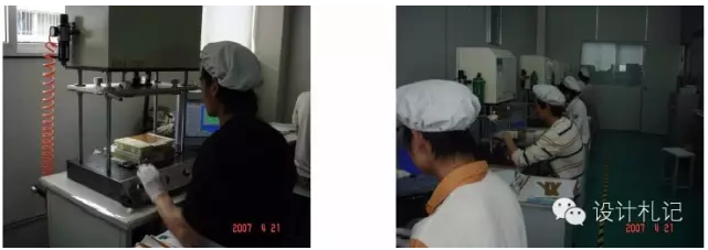
13. Inspection
Inspection items: appearance, size, reliability
Testing tools: secondary element, micrometer, caliper, magnifying glass, tin furnace, tensile force
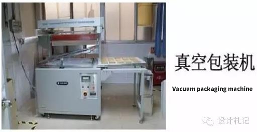
14. Packing operation method:
(1) Plastic bag + cardboard
(2) Low adhesion packaging materials
(3) Standard vacuum box
(4) Special vacuum box (antistatic grade)