In different application scenarios, high-speed board design needs to closely fit its core functions and physical limitations, showing obvious differentiated emphasis. As the nerve center of the system, the backplane carries the heavy responsibility of connecting many daughter cards and realizing high-speed data exchange. The core challenge of this type of high-speed board design is to overcome the signal integrity problems caused by ultra-high density interconnection. It places special emphasis on strict impedance control to match high-speed signal channels, and has almost harsh requirements on the selection, layout and back drilling process of connectors. Reflection and crosstalk must be minimized to ensure data reliability and clock synchronization under long-distance transmission. At the same time, the huge physical size and complex stacking structure of the backplane also put forward unique requirements for heat dissipation and mechanical strength.
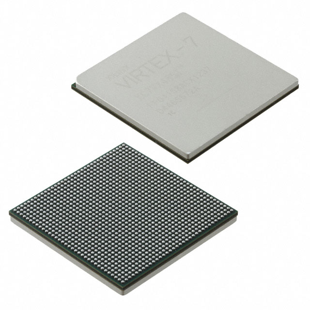
For line cards (or business cards), the high-speed board on them is directly responsible for the transmission, processing and forwarding of signals. This type of design focuses on optimizing the transmission path of signals from interfaces to processing chips. High-speed boards must carefully lay out high-speed differential pair lines, precisely control their equal length, equal distance and spacing to minimize inter-symbol interference and signal distortion, and ensure data fidelity at high frequencies (such as 25G+). Power integrity and low-noise power supply are another key, and an extremely "clean" energy source must be provided for high-speed chips through optimized stacking, a large number of decoupling capacitors and possible split power layers. In addition, the heat dissipation density is usually higher, and a heat sink or even a duct design is required.
As for optical modules, the high-speed boards inside them realize electro-optical/photoelectric conversion in an extremely compact space. The primary focus of the design is highly compressed to the ultimate balance between extreme miniaturization and high-frequency performance. The area of high-speed boards is very expensive, the number of wiring layers is limited, and the RF design concept is widely borrowed. It is necessary to finely simulate and optimize the microstrip/stripline structure, pay special attention to the high-frequency skin effect and dielectric loss, and cleverly use mixed substrate materials (such as FR4 combined with Rogers) to meet stringent insertion loss and return loss indicators. Its design must also solve the electromagnetic compatibility problem between high-speed chips, drive circuits and lasers/detectors at extremely short interconnection distances. In summary, when designing high-speed boards, the backplane focuses on the stability of large-size, high-density interconnections, the line card emphasizes the signal quality and power supply guarantee of the integrated path, and the optical module pursues high-frequency performance and heat dissipation coordination under the limit of miniaturization.