The semiconductor industry mainly focuses on integrated circuits, consumer electronics, communication systems, photovoltaic power generation, lighting applications, high-power power conversion, and other fields. From the perspective of technology or economic development, the importance of semiconductors is enormous
Most electronic products today, such as computers, mobile phones, or digital recorders, have a very close relationship with semiconductors as their core units. Common semiconductor materials include silicon, germanium, gallium arsenide, etc. Among various semiconductor materials, silicon is the most influential in commercial applications.
Semiconductors refer to materials with conductivity between conductors and insulators at room temperature. Due to its widespread application in radios, televisions, and temperature measurement, the semiconductor industry has enormous and ever-changing development potential. The controllable conductivity of semiconductors plays a crucial role in both technological and economic fields.
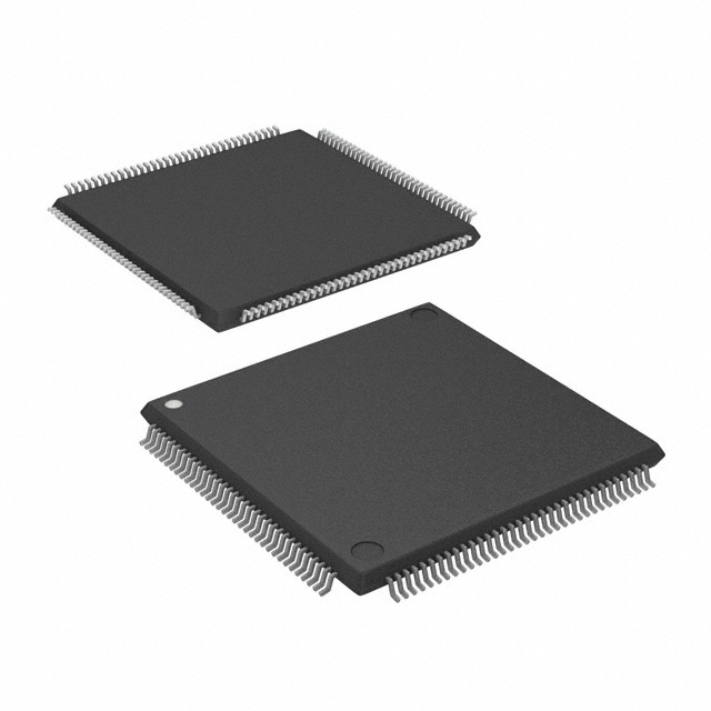
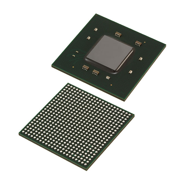
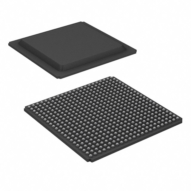
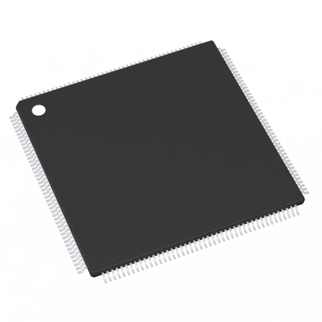
The upstream of the semiconductor industry are IC design companies and silicon wafer manufacturing companies. IC design companies design circuit diagrams according to customer needs, while silicon wafer manufacturing companies manufacture silicon wafers using polycrystalline silicon as raw material. The main task of midstream IC manufacturing companies is to transplant the circuit diagrams designed by IC design companies to the wafers manufactured by silicon wafer manufacturing companies. The completed wafers are then sent to downstream IC packaging and testing factories for packaging and testing.
The substances in nature can be divided into three categories based on their conductivity: conductors, insulators, and semiconductors. Semiconductor materials refer to a type of functional material with conductivity between conductive and insulating materials at room temperature. Conduction is achieved through the use of two types of charge carriers, electrons and holes. The electrical resistivity at room temperature is generally between 10-5 and 107 ohms · meters. Usually, the resistivity increases with increasing temperature; If active impurities are added or irradiated with light or radiation, the electrical resistivity can vary by several orders of magnitude. The silicon carbide detector was manufactured in 1906. After the invention of transistors in 1947, semiconductor materials, as an independent field of materials, have made great progress and become indispensable materials in the electronic industry and high-tech fields. The conductivity of semiconductor materials is highly sensitive to certain trace impurities due to their characteristics and parameters. Semiconductor materials with high purity are called intrinsic semiconductors, which have high electrical resistivity at room temperature and are poor conductors of electricity. After adding appropriate impurities to high-purity semiconductor materials, the electrical resistivity of the material is greatly reduced due to the provision of conductive carriers by impurity atoms. This type of doped semiconductor is often referred to as impurity semiconductor. Impurity semiconductors that rely on conduction band electrons for conductivity are called N-type semiconductors, and those that rely on valence band hole conductivity are called P-type semiconductors. When different types of semiconductors come into contact (forming PN junctions) or when semiconductors come into contact with metals, diffusion occurs due to the difference in electron (or hole) concentration, forming a barrier at the contact point. Therefore, this type of contact has single conductivity. By utilizing the unidirectional conductivity of PN junctions, semiconductor devices with different functions can be made, such as diodes, transistors, thyristors, etc. In addition, the conductivity of semiconductor materials is highly sensitive to changes in external conditions such as heat, light, electricity, magnetism, etc. Based on this, various sensitive components can be manufactured for information conversion. The characteristic parameters of semiconductor materials include bandgap width, resistivity, carrier mobility, non-equilibrium carrier lifetime, and dislocation density. The bandgap width is determined by the electronic state and atomic configuration of the semiconductor, reflecting the energy required for valence electrons in the atoms that make up this material to excite from the bound state to the free state. Electrical resistivity and carrier mobility reflect the conductivity of a material. The non-equilibrium carrier lifetime reflects the relaxation characteristics of internal carriers in semiconductor materials transitioning from non-equilibrium state to equilibrium state under external effects (such as light or electric field). Dislocation is the most common type of defect in crystals. The dislocation density is used to measure the degree of lattice integrity of semiconductor single crystal materials, but for amorphous semiconductor materials, this parameter is not present. The characteristic parameters of semiconductor materials can not only reflect the differences between semiconductor materials and other non semiconductor materials, but more importantly, they can reflect the quantitative differences in the characteristics of various semiconductor materials and even the same material in different situations.